

In my previous post I introduced the first two steps of a three step process for calculating the required op amp bandwidth for your transimpedance amplifier. In this post I’ll explain the final step and introduce a design example using this process.
Step 3: Calculate the required op amp gain bandwidth product.
A basic stability analysis will reveal the logic behind this step, but if you just want the calculation you can skip to equation 5. Figure 1 shows the TINA-TI™ circuit used for the analysis. The feedback loop is broken with a large inductor (L1) and a voltage source is ac coupled to the loop through a large capacitor (C1). The loop is broken at the op amp output so that the effects of the input capacitance are included in the analysis. An ac transfer characteristic is performed and the post-processor is used to generate the open-loop gain (AOL) and noise gain (1/β) curves (Figure 2).
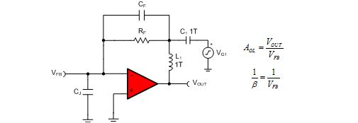
Figure 1: Breaking the feedback of a transimpedance amplifier and generating AOL and 1/β curves.
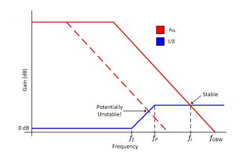
Figure 2: AOL and 1/β plot for a typical transimpedance amplifier circuit.
On the 1/β curve there are 3 points of interest. First, there is a zero at the frequency:

Above this frequency, the 1/β curve will increase a rate of 20dB per decade. Next, there is a pole, at the frequency:

which will cause the 1/β curve to “flatten out.” Finally, the 1/β curve intersects the AOL curve at the frequency:

In equation 5, fGBW is the unity gain bandwidth of the op amp. In order to maintain stability, the AOL curve must intersect the 1/β curve when the 1/β curve is flat (assuming a unity gain stable op amp). If the AOL curve intersects the 1/β curve when the 1/β curve is rising, as shown by the dashed line in Figure 4, the circuit may oscillate. This gives us the rule:
Inserting the equations for fI and fp into this rule and solving for unity gain bandwidth, we arrive at a useful equation:
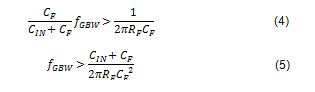
Equation 5 eliminates one of the mysteries when selecting an op amp for your transimpedance amplifier design. Choosing an op amp with adequate bandwidth not only ensures you have sufficient signal bandwidth, but also helps to avoid potential stability headaches!
Design Example
Now I’ll apply this process to a design example and compare the performance of the circuit using two op amps. One op amp will meet the gain bandwidth requirements we calculate and the other will not. The requirements for this design example are given in table 1.
Table 1: Example performance requirements for a transimpedance amplifier

To start, we calculate the maximum feedback capacitance for the circuit to be stable and still meet our bandwidth goal:

Next, we determine the capacitance at the inverting input of the amplifier. Because we haven’t selected an op amp yet for our circuit we do not know the values of CD and CCM2. Remember that I suggested 10pF as a reasonable guess for this capacitance in Part I.

Finally we can calculate the gain bandwidth requirements for the op amp:

For this example, I’ll compare the two op amps shown in table 2:
Table 2: Gain bandwidth product comparion of two op amps for the design example.

From our previous calculations, we know that one of these op amps, the OPA313, does not have sufficient bandwidth for our circuit. But how does this actually affect the operation of the circuit?
Read part 3 which is coming soon to find out!


