This thread has been locked.

If you have a related question, please click the "Ask a related question" button in the top right corner. The newly created question will be automatically linked to this question.

TAS5766 Volume up/Volume down register and Necessary register set page

Other Parts Discussed in Thread: TAS5766M, TAS5766MDCAEVM

Dear all,
I have 2 qestions,especially in TAS5766 register setting,need your support ,thanks~
 
1.after read TAS576x technique document(TAS576xM 2x50W/4Ω PurePath Smart Amp) ,except
  Analog gain can controlled by Ra(to GND) and Rb(to GVDD) ;
  DAC gain controlled by Page 1/Register2(HEX 0x2) and Page 1/Register 7(Hex 0x7) ,
  Does any actual register exist for volume control ?

2.I got TAS5766 parameter file (TAS5766.h) from Learning Board and PurePath GUI ,
  there are almost 4 thousand I2C commands which I need to write to TAS5766,I prepare to send
  the 4 thousand I2C commands at system initialize stage ,but I think sending 4 thousand of I2C commands
  will take a little of time ;
  the 4 thousand commands includes :
 
  page 44 ~ 52
  page 62 (Coefficient Memory B)
  page 63 ~ 70
  page 152 (Instruction Memory)
  page 153 ~ 169
  page 0
  page 1
 
  In order to saving system booting up time,
  Does all upper pages I need to program at system initial stage ?

  • Hi Joi,

    I think SLAA626A has the info that you are looking for. Please search for volume control in the apps note which has an example.

    reg,

    Paul Chen

    Audio Apps.

  • Hi Joi,

    Please refer to these wiki pages:

    http://e2e.ti.com/support/amplifiers/audio_amplifiers/w/design_notes/2761.how-to-implement-smart-amp-code-into-an-end-system.aspx

    http://e2e.ti.com/support/amplifiers/audio_amplifiers/w/design_notes/2845.tas5766m-effects-of-power-cycling-on-memory.aspx

    As explained in the Smart Amp Design Guide document, you can use .reg files to define how the TAS5766M contents will be dumped into a header file. Just set the Burst parameter in the dump tool to 120 to reduce code size.

    Below are example .reg files that you can use:

    2451.SLAAxxx [PurePath™ Smart Amp for Laptops]_20141010.zip

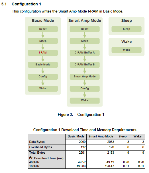
    We're working on an app note to address this kind of applications where time and size is important, but it might take a couple of weeks to get it released. The file I provided has 4 configurations. I think something similar to what you see below is what you need.

    Regards,

    J-

  • Hi J Arbona,

    Thanks for your information ,the information for us is very useful,further questions need your confirm ,

    (1) as information you provide ,
       1.1. when programming TAS5766 as Basic Mode ,except writing page0/page 1 registers ,we need to writing Instruction Memory (page 152 ~ page 169) additionally ?
       1.2. when programming TAS5766 as SmartAMP Mode ,except writing page0/page 1 registers ,we need to writing C-MEM A(page44 ~ page52), C-MEM B(page62 ~ page70),
                                even Instruction Memory (page 152 ~ page 169) additionlly ?

    (2) from your script file ,I can know that page0/Register61(0x3D) and page0/Register62(0x3E) can control Digital gain ,right ?
        Is there any techique document descript this ,because from SLAS965B(TAS576xM 2x50W/4Ω PurePath™ Smart Amp) ,I cannot see this
        register

    (3) Because in our product ,we make TAS5766 as I2S slave ,from the route path captured from SLAS965B


    Does SRCDAC register exist ? such that I can choice BCK acting as DAC source ;
    (about route path,I can only see Page 0/Register 13 (0x0D) [PLL  reference clock choice SCK or BCK] )

  • Hi J Arbona,

    thanks for your information ,the information is very useful for us ,

    sorry ,I have further questions need your confirm ,

    (1) as information you provide ,
       1.1. when programming TAS5766 as Basic Mode ,except writing page0/page 1 registers ,we need to writing Instruction Memory (page 152 ~ page 169) additionally ?
       1.2. when programming TAS5766 as SmartAMP Mode ,except writing page0/page 1 registers ,we need to writing C-MEM A(page44 ~ page52), C-MEM B(page62 ~ page70),even Instruction Memory (page 152 ~ page 169) additionlly ?

    (2) from your script file ,I can know that page0/Register61(0x3D) and page0/Register62(0x3E) can control Digital gain ,right ?
        Is there any techique document descript this ,because from SLAS965B(TAS576xM 2x50W/4Ω PurePath™ Smart Amp) ,I cannot see this register 

    (3) Because in our product ,TAS5766 acts as I2S slave device ,refer to SLAS965B((TAS576xM 2x50W/4Ω PurePath™ Smart Amp) ,the route path diagram :

    Does SRCDAC register exist ? such that I can choice BCK acting as DAC source ;
    (about route path,I can only see Page 0/Register 13 (0x0D) [PLL  reference clock choice SCK or BCK] )

    thanks ~

  • about question (3) the route path is :

  • sorry ,the route path is following:

  • Hi Joi,

    "   1.1. when programming TAS5766 as Basic Mode ,except writing page0/page 1 registers ,we need to writing Instruction Memory (page 152 ~ page 169) additionally ?"

    The reason we are writing I-RAM on Basic mode is to split the download time into two, so Smart Amp mode download is faster the first time. But I-RAM is not necessary for Basic Mode, only for Smart Amp mode. If you are OK with 100ms or so for initialization, then you can use Configration #3, which has I-RAM written during Smart Amp mode. See the .reg file for Configuration #3 for details.

    "  1.2. when programming TAS5766 as SmartAMP Mode ,except writing page0/page 1 registers ,we need to writing C-MEM A(page44 ~ page52), C-MEM B(page62 ~ page70),even Instruction Memory (page 152 ~ page 169) additionlly ?"

    Correct. C-RAM and I-RAM are used for Smart Amp mode and need to be downloaded with the correct data. However, as you will notice that in Basic Mode in any configuration a software reset is performed first. This will clear C-RAM to default.However, I-RAM is retained even if you reset. I-RAM would be cleared only if DVDD is removed.

    You can reduce the download by 256x4 bytes by skipping C-RAM B download. However, in such case, you will not be able to change volume on the fly.

    "(2) from your script file ,I can know that page0/Register61(0x3D) and page0/Register62(0x3E) can control Digital gain ,right ?
        Is there any techique document descript this ,because from SLAS965B(TAS576xM 2x50W/4Ω PurePath™ Smart Amp) ,I cannot see this register "

    It will be shown when the app note is released. Below is an example. This register must be 0dB when using Smart Amp mode (the script will do that for you).

    0dB = 00110000

    -0.5dB = 00110001

    -103dB = 11111110

    "(3) Because in our product ,TAS5766 acts as I2S slave device ,refer to SLAS965B((TAS576xM 2x50W/4Ω PurePath™ Smart Amp) ,the route path diagram :

    Does SRCDAC register exist ? such that I can choice BCK acting as DAC source ;
    (about route path,I can only see Page 0/Register 13 (0x0D) [PLL  reference clock choice SCK or BCK] )"

    You can see this in this in the Config Block where PLL source is BCLK. So it is already configured this way. Note that BCLK must be 32*FS or 64*FS for this to work.

    Regards,

    J-


  • Hi J Arbona,

    Thanks for your detail explain,it really answer my question ~ ,

    another question need your help ,In my project use case ,We have another CPU acts as I2S master ,and TAS5766 acts as I2S slave ,CPU will provide fixed frequency LRCLK 44.1Khz ,fixed frequency BCLK = 64 * LRCLK ;and we don't use SCK ,but only 3 wires (LRCLK,BCLK,DIN) ; after refer to SLAS965B (Table 8. Recommended Clock Divider Settings for PLL as Master Clock) ,RSCLK = 64 filed,a little confuse of Clock Divider value setting ;

    if CPU acts as I2S master and provide fixed frequency LRCLK 44.1Khz ,fixed frequency BCLK = 64 * LRCLK ;TAS5766 acts as I2C slave ,and use BCLK route to PLL reference clock ,refer to SLAS965B (Table 8. Recommended Clock Divider Settings for PLL as Master Clock) ,Is the following register setting right ?

    page 0/Register4 = 0x01;

    page 0/Register20(0x14) = 0x0; (PLL P=1)

    page 0/Register21(0x15) = 0x10 ; (PLL J= 16)

    page 0/Register22(0x16) = 0x00; (D= 0)

    page 0/Register23(0x17) = 0x00;

    page 0/Register24(0x18) = 0x01; (PLL R= 2)  

    page 0/Register13(0x0D) = 0x10 ; (The PLL reference clock is BCK)

    page 0/Register27(0x1B) = 0x01 ;(DSP Clock divider is divided by 2)

    page 0/Register28(0x1C) = 0x0f ;(DAC Clock divider is divider by 16)

    page 0/Register29(0x1D) = 0x03; (NCP Clock divider is divider by 4)

    page 0/Register30(0x1E) = 0x07;(OSR Clock divider is divider by 8)

    le 

  • Hi Jeffrey,

    You basically need to write the register location in CRAM_A, swap buffers and re-wrtie the same data to CRAM_A location again.

    For example:

    w 98 00 2c # Page 44
    w 98 88 40 00 00 # Write P44/R8,9,10,11 coefficients. Note that for TAS5766M, the MSB of reg addr must be '1' for burst writes.
    w 98 00 2c
    w 98 01 05 # Swap buffers
    w 98 88 40 00 00 # Re-write same data again.

    You can find detailed information here: http://www.ti.com/lit/pdf/slaa425

    Regards,

    J-

  • Regarding digital volume control in Page 0, you have to be careful since this is a post-processing gain control. Refer to the Smart Amp User Manual in the TAS5766SW-SA page of ti.com/mysecuresoftware.

    J-
  • HI Jeffrey,

    "What's the meaning of " the Smart Amp User Manual in the TAS5766SW-SA page of ti.com/mysecuresoftware." ? 
    By the way, Is it necessary to Sleep and Wake procedures 'before' and 'after' your reference code ?
    Refer to the SLAA425D. it mentioned two families devices. But I can NOT find the TAS5766M chip in the list. 
    Why did TI not provide well organized document to customers ?"

    We keep our Smart Amp software and documentation on a website called mySecureSoftware. Access to these are restricted for Smart Amp devices so you cannot simply get the software and documentation from a link.

    We have a Smart Amp Overview document that explains what I mention above: www.ti.com/.../slaa625.

    Inside the TAS5766MSW-SA page in mySecureSoftware, you will find a Smart Amp User Manual where step-by-step information about Smart Amp development is provided.

    Regards,

    J-

  • Hi Jeffrey,

    "Regarding SLAU645 (Easy Demo User Manual), it mentioned TAS5766M and AIC3262. Can you release the source code to us as reference ?"

    The software (source code, process flow, etc) is in the bottom of the tool page: http://www.ti.com/tool/TIDA-00609

    Here is a direct link: www.ti.com/.../tidcaj4

    Regards,

    J-

  • Hi Jeffrey,

    "We struggled with TAS5766M volume control issue for a couple of days and

    can NOT understand why TI can not provide enough information to customers."

    You would need to click the More Info button in the TAS5766MDCAEVM page as explained here: www.ti.com/.../slaa625

    That will give you access to all the documentation.

    Regarding the access to PurePath Studio and TAS5766MSW-SA, I just gave you access to it. In general, we don't provide access to non-corporate email accounts, which is the reason why Don rejected it.

    Regards,

    J-

  • Hi Jeffrey,

    If you write CRAM in Sleep (RQST = 1), you would need to write to both C-RAM Buffer A and B locations (i.e. Page 44.. and Page 62..).

    If you write CRAM while running (Wake) and in adaptive mode, you only need to write the the C-RAM Buffer A location with a buffer swap in between (buffer swaps only work in wake state and not in sleep state).

    More details are here:

    e2e.ti.com/.../2845.tas5766m-effects-of-power-cycling-on-memory

    Examples:

    --------------

    If device is in Sleep state:

    AUDIO_AmpSleep();

    I2C_TxAddrByte(AUDIO_MAD, 0x00, 0x2C); // Page 44
    I2C_TxAddrBulk(AUDIO_MAD, 0x80 | 0x08, 3, (UI8 *)au8P2C_R08_R0A + u8Idx); // R08 - R0A

    I2C_TxAddrByte(AUDIO_MAD, 0x00, 0x3e); // Page 62
    I2C_TxAddrBulk(AUDIO_MAD, 0x80 | 0x08, 3, (UI8 *)au8P2C_R08_R0A + u8Idx); // R08 - R0A

    AUDIO_AmpWake();

    -----------------

    If device is in Wake state:

    AUDIO_AmpWake();

    I2C_TxAddrByte(AUDIO_MAD, 0x00, 0x2C); // Page 44
    I2C_TxAddrBulk(AUDIO_MAD, 0x80 | 0x08, 3, (UI8 *)au8P2C_R08_R0A + u8Idx); // R08 - R0A

    I2C_TxAddrByte(AUDIO_MAD, 0x00, 0x2C); // Page 44 (optional because it is already on page 44).
    I2C_TxAddrByte(AUDIO_MAD, 0x01, 0x05); // Swap Buffers

    I2C_TxAddrByte(AUDIO_MAD, 0x00, 0x2C); // Page 44
    I2C_TxAddrBulk(AUDIO_MAD, 0x80 | 0x08, 3, (UI8 *)au8P2C_R08_R0A + u8Idx); // R08 - R0A

    ------------------

    A value of 0x400000 corresponds to 0dB gain. A value of 0x200000 corresponds to -6dB and so forth.

    I would not recommend changing any other register in C-RAM on the fly other than P44_R8-11 or P62_R8-11.

    Regards,

    J-

  • Jeffrey,

    Go to the End-System Integration page, and select In-System Tuning. You can use the PurePath Console Motherboard by connecting to the I2C test points. More information is on the Smart Amp User Manual.

    Regards,

    J-

  • Jeffrey,

    That debugger is not compatible with PPC.

    J-