This thread has been locked.

If you have a related question, please click the "Ask a related question" button in the top right corner. The newly created question will be automatically linked to this question.

TAS5538/TAS5624A Pop Noise Issue

Other Parts Discussed in Thread: TAS5538, TAS5624A

Hi,

Could you please tell us your advice regarding TAS5538 and TAS5624A as below?

Q1. 8Interchannel Channel Delay Register for TAS5538
(a) Registers for AD Mode, BD Mode and Ternary
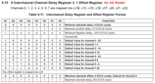
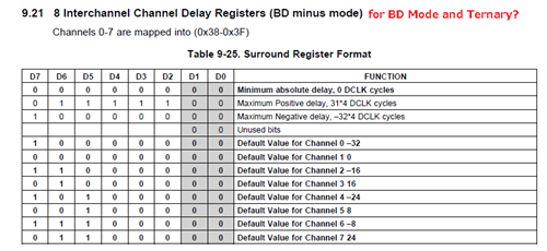
We believe that the interchannel delay registers are mapped into 0x1B to 0x22 for AD mode and are mapped into 0x38 to 0x3F for BD mode and ternary.
Is our understanding correct?

(b) Delay Adjustment of Each Positive Output and Negative Output for TAS5538
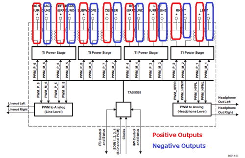
Can we independently adjust the delay of each positive output and negative output?
Please let us know that setting procedure if possible.

Q2. Inter Mux Registers for TAS5538(0x30 to 0x33)
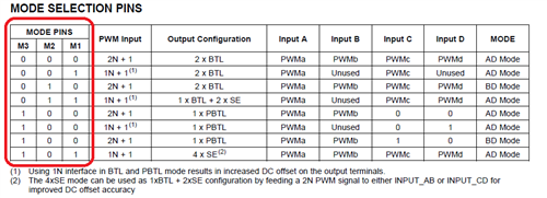
Could you please tell us the logic to set AD mode and BD mode?
We believe that AD mode should be set D7 and D3 to 0b and BD mode should be set D7 and D3 to 1b.
Is our understanding correct?

Q3. All Registers which Should be Changed to Set BD Mode for TAS5538
Could you please tell us all registers which should be changed to set BD mode?

Q4. Connected Method of Mode Pins for TAS5624A
Could you please tell us whether the mode pins are directly able to be connected to DVDD or GND without the pull-up/down resistors?
We believe that the mode pins are directly able to be connected to DVDD or GND.
Is our understanding correct?

Q5. Pop Noise for TAS5538 and TAS5624A
The pop noise occurred with the test board of our customer if the mute pin is asserted to high or the soft mute(0x0F) is asserted to high for TAS5538.
Could you please tell us the workaround to improve that issue?

Best Regards,
Kato

  • Hi, Kato-san,

    Tuan will get back to you on this.

    reg,

    Paul.

  • Hi Paul-san,

    Thank you for your response.
    I am looking forward to hearing from Tuan-san.

    Best Regards,
    Kato

  • Hi Kato-san:

    As indicated by your statement, the questions above are for addressing the pop noise problem.  Let me go ahead and address that first in this reply.

    1.  Please set the modulation mode to BD modulation

    0x30 89 (channel 1 and 2 BD mode)

    0x31 AB (channel 3 and 4 BD mode)

    0x32 CD (channel 5 and 6 BD mode)

    0x33 EF (channel 7 and 8 BD mode)

    2.  Change the volume slew rate to the longest time in register 0xD0

    Also,  I have the scope captures you sent.  The order should be de-assert reset, then de-assert power down.  De-asserting mute is the last step.

    Best regards,

    Tuan

  • Hi Tuan-san,

    Thank you for your cooperation.
    I have reported the information which I have obtained from you regarding the pop noise and customer's schematic and am looking forward to hearing from you about the remaining items of Q1(a), Q1(b) and Q3.

    Best Regards,
    Kato

  • Hi Tuan-san,

    I have evaluated the evm of TAS5538+TAS5624A for Q1(a) and Q1(b), obtained the results as below.
    For AD mode, it is possible to set each channel phase by using the address of 0x1b~0x22.
    For BD mode, it is possible to set the phase of each positive output by using the address of 0x1b~0x22, to set the phase of each negative output by using the address of 0x38~0x3f.
    By the way, I am looking forward to hearing from you about the remaining item of Q3.

    Best Regards,
    Kato

  • Hello Tuan-san,

    Can you update this post for Kato-san?

    Or we can be ready to have a conf call.

    Thank you and best regards,

    Daisuke KAWASAKI

  • Hi Kato-san:
    Q1a - 1Bh to 22h are for AD and BD modulation ICD settings and 38h to 3F are for Ternary modulation ICD settings.
    Q1b - In some TI modulators it is possible to adjust the Inter Channel delay (TC delay) giving different results in terms of dynamic range and THD in a system.
    The TC delay is defined as the delay from one half bridge positive output to another channel positive output. Negative output cannot be adjusted.
    Because of cross coupling between the channels in the power stage of the amplifier each PWM transition will disturb the other channels resulting in timing uncertainties. This will result in increased noise and increased THD.
    Many factors have influence on this deterioration of the system performance. Cross coupling is different in each power stage. Cross coupling also depends on the physical distance between the channels on the PCB and the amount of filtering circuits added to the supply rail between channels. So an individual optimization is needed for each application.
    TI strongly recommends using default values for these parameters. In most cases, adjustments to these values are not necessary.
    Best regards,Tuan
  • Q3BD mode I2C settings:Reg Value0x30 0x890x31 0xAB0x32 0xCD0x33 0xEF
    AD mode I2C settings:0x30 0x010x31 0x230x32 0x450x33 0x67Best regards,Tuan
  • Hi Tuan-san,

    Thank you for explaining so politely.
    I understood and will contact you again if I have additional questions.

    Best Regards,
    Kato