This thread has been locked.

If you have a related question, please click the "Ask a related question" button in the top right corner. The newly created question will be automatically linked to this question.

TPA3251D2 2nd order distortion products.

Other Parts Discussed in Thread: LME49724, LM46002

Greeting chaps, I managed to snag a sample from a kind individual over on one of the DIY forums and have got a stereo board up and running.

Upon measuring the device however I am seeing rising 2nd order distortion towards low frequencies. This gets significantly worse the higher the output power.

Prior to the device I am using an LME49724 to perform single ended to balanced conversion. I have measured this in isolation and know that this is not the source of the issue.

12V supplies are provided by two LT4032s. One powers the opamps, one the 12V section of the amplifier. An LM46002 provides pre regulation from the power stage power rail. Currently I am powering this from a number of lithium ion cells @ around 25V. I have tried other PSUs but the problem remains, so I doubt it's that.

The performance is otherwise as expected, all the other harmonics are very low, only the 2nd order jumps up and rises towards low frequencies.

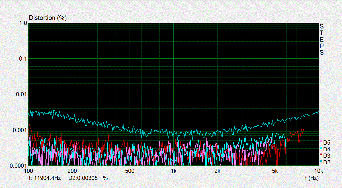
Here is an example at 2.8VRMS into a 9.4 ohm load.


Increasing the output power causes the issue to get worse in magnitude and start at higher frequencies. All other harmonics remain unaffected and both channels perform identically. - The 2nd order rise is significantly worse if only one channel is measured too, ie having the amplifier set to BTL mode, but only measuring a single half. And this is a matter of current, rather than voltage, as the issue is not present when no load is connected.


Without you guys needing to wrack your brains too hard over this, is there a known mechanic that might be the cause of this? I have built my design to the recommended circuit diagram in the data sheet, and description therein, but I am wondering if certain components could be the cause? The output inductors are from Ice Components, the main LC caps are polypropylene and the other snubber caps are COG.

Usually when only a single harmonic is present it points towards something specific being the issue.


Many thanks,


Matt.

  • OK so update. It isn't the output inductors as I tried some beefier ones to the same effect.

    I tried adding in more ceramic decouplers to the power stage pins, increasing the effective capacitance and this had no effect.

    I tried increasing c start, which as I've read, could improve psrr this also had no effect.

    The most important thing I figured out is this.

    If, when in BTL mode, one channel is driven with a load connected to it, then the other channel is driven but with no load connected, the channel with no load connected to it shows the same increase in 2nd harmonic too.

    This is odd because it isn't delivering any current but implies that the contamination affects both channels equally.

  • Well to answer my own questions it seems like this may be PSU related after all. I figured batteries would give a nice low impedance supply I guess they do not.

    Attaching some large bulk capacitance to the input rail of the PCB appears to have helped considerably.

  • Okay so it isn't the PSU, it has some effect but I think it is more mitigating another larger general issue. What's odd is this is only second order.

    I had a third order only issue with the feedback resistor in a class AB amp at one point but I have very little knowledge as to what causes class D nonlinearities.

  • Hi Matt,

    Thanks for sharing your plots and detailed description of this issue. When driven by a balanced input on an AP analyzer, the TPA3251D2 has very low 2nd order harmonic distortion in BTL mode (lower than 3rd order). Since there is a very large amount of loop gain at low frequencies, the part itself has no mechanism for having a rise in THD at low frequency. The rise at low frequency is most likely external issue. One possible source of D2 is a PSU ripple disturbing the reference voltage or the supplies or grounds of the single-ended to differential conversion preamplifier. Layout could be critical in keeping the preamp as clean as possible.

    You mentioned that you had measured the THD of the SE-to-DIFF circuit by itself. It looked OK. Could you try measuring the output of that circuit while it is driving the TPA3251D2 under load? I hope to hear more about this as you continue to experiment.

    Regards,

    Jeff

  • Hello Jeff thanks for your response as this will most certainly give me something to go on.

    I had assumed that even order distortion products would be lower than odd due to the balanced nature of the amplifier so the higher than normal levels of 2nd order were a little curious.

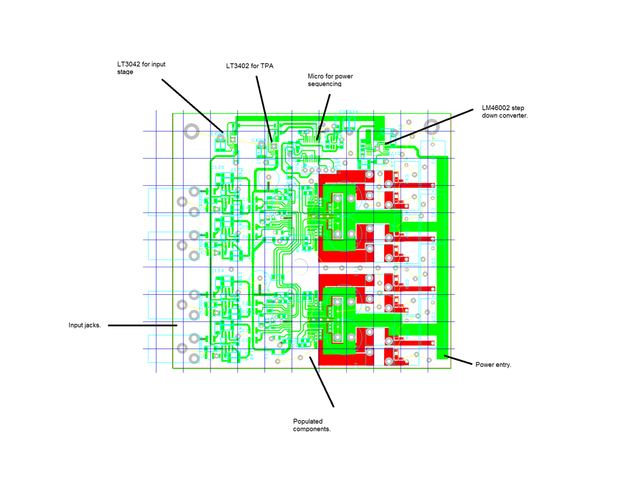
    Attached is an image of the board layout with some annotations attached.

    This is second iteration that I have tried, just to see if any differences were to be had. My first implementation didn't use any traces on the reverse side of the board so that a continuous ground plane would be present. On the second iteration I decided to try routing the traces concerned with the amplifiers outputs to the rear of the board. Both designs performed pretty much identically. The copper pour areas have been removed for clarity but care has been paid to the layout to ensure that there is a relatively clean path back to the PSU entry point for the return current from the TPA. As I only have one TPA at this moment in time I cannot perform comparisons to the upper and lower chips, which could be quite useful in potentially diagnosing the cause.

    The main idea behind my layout was to keep the high current, high rise time current loops to the bottom right hand side of the PCB with the return take off point being the copper plane beneath the power entry point. The rest of the components being placed 'downstream' to help with wayward currents that could otherwise disturb sensitive parts of the circuitry.

    The most interesting thing that you've mentioned is with the voltage reference within the TPA. I say this because both channels are affected similarly even with a load connected to a single channel. The input stages are independent of one another and I would expect to see some differences between the two channels if this were the case, but for the most part I do not.

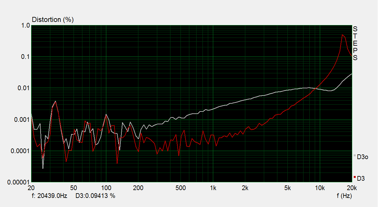
    For example here is a plot of the third harmonic. This is with the amplifier driving 4 watts into my 4.7 ohm dummy load.

    The dark red line shows the response of the channel that has no load connected, whereas the other one is with the load connected. Quite clearly there is a lot of difference here, as one would expect, one output channel is doing nothing whereas the other one is working hard.

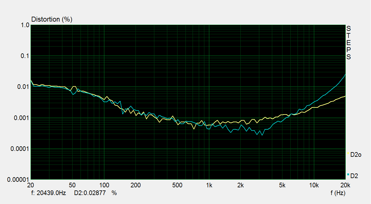
    Here is the second order for comparison.

    Where both channels converge between 1 and 2 kHz and then track each other almost perfectly down until 20Hz.

    I will most certainly try and take measurements of after the differential stage with the amplifier with and without load.

  • Okay so interesting. I tried doing the measurements of the differential stage to get a better understanding of what's going on.


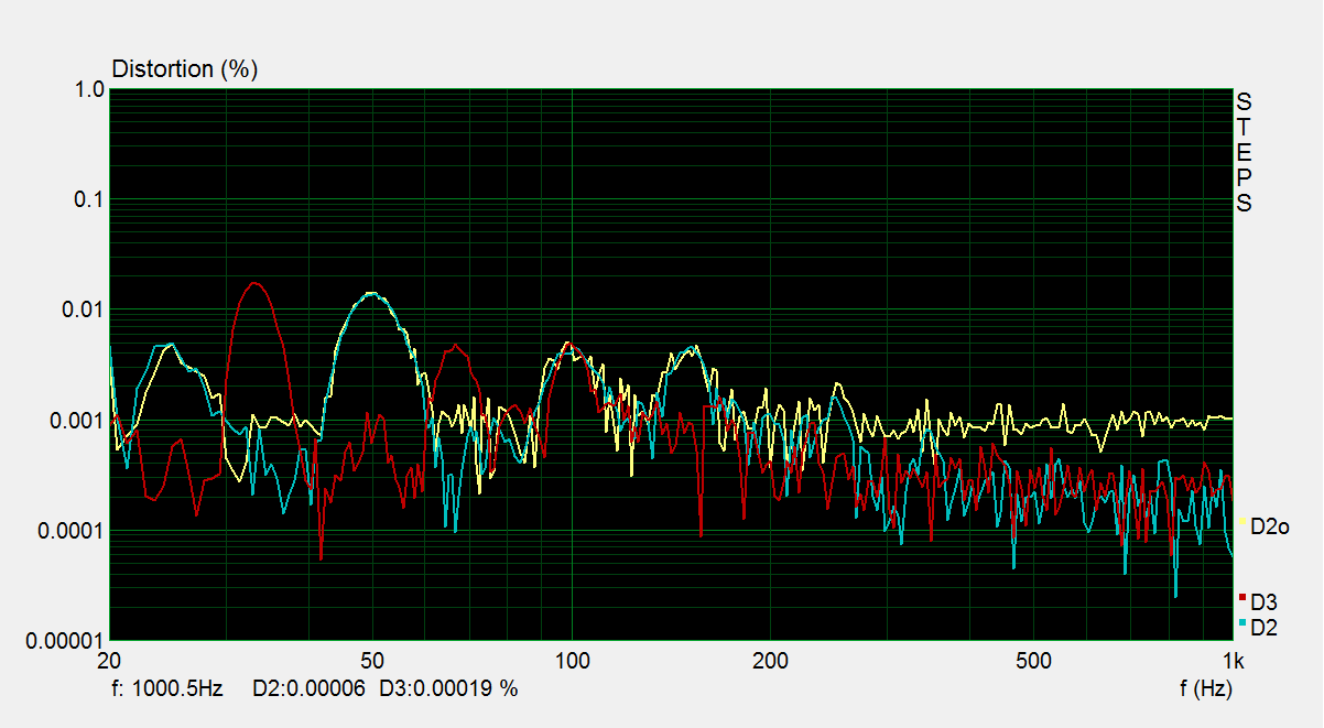
    Here we have an image showing just that. The dark red line is the 3rd harmonic and the green line is the 2nd. These are for the output of the differential stage preceding the TPA without any load connected. The yellow line is what happens to the 2nd order products when the load is connected a huge increase. The load and measurement conditions were the same as the measurements provided above.

    Now what is interesting is this.

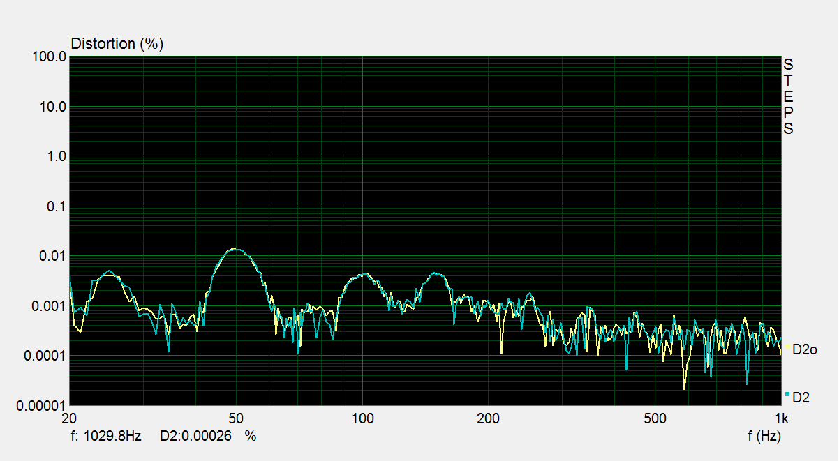
    This is what happens if I remove the coupling caps present on the other input. One trace is with the other channel driving the 4.7R load and one is without. No difference. Connect the coupling caps and everything falls to pot again. I'd say this indicates that the differential input stage is working perfectly fine in isolation, it's when it's connected to the TPA that things start to look bad.

  • I thought I'd just point out that the spikes coming in at low frequencies are mains related hash.

    I will also clarify that the last image above is with channels C and D operating as intended and driving the 4.7 ohm load. Channels A and B had the coupling caps before the TPA inputs removed and I measured the output of the differential input stage directly without it being connected to the TPA. This resulting in the curves above. One of them is without channels C and D driving a load and the other is with C and D driving a load. If I put back the coupling caps and measure A and B again the 2nd order shoots up to like the yellow trace in the first image of the above post.