This thread has been locked.

If you have a related question, please click the "Ask a related question" button in the top right corner. The newly created question will be automatically linked to this question.

TAS5766M: Solder Paste Requirements

Part Number: TAS5766M

I have a customer who needs some guidance on the solder paste requirements for the TAS5766M.  In particular, do we recommend 50% minimum solder paste coverage over the exposed pad?  Their manufacturing arm is referencing SLUA271A (http://www.ti.com/lit/an/slua271a/slua271a.pdf ) to justify 50% coverage.  SLUA271A states:


Typically, the solder-paste coverage is approximately 50% to 70% of the pad area (see Figure 11).

Designing an aperture that prints solder 1:1 with the exposed pad results in excessive metal volume that

will “float” the part, causing opens and other manufacturing defects. In addition, the amount of voiding post

reflow in the thermal pad solder joint should not exceed 50% in high power applications (to be verified

using an x-ray). Based on a JEDEC High K board stackup, 25% has been determined to be a point of

diminishing thermal performance returns, but TI prefers a limit of 50% to be set (reference JESD51-7).

First, is this application note applicable to the TAS5766M QFN package which is substantially bigger.

Second, its unclear what 50% - 70% would realistically look like.  I have some confidential pics I can show offline.

Please let me know who I can talk to about this ASAP bec they are in the process of building this up now!

Thanks, John Garrett, TI-AFA 

  • Hello John!

    I'll send you a separate email to cover this.  Thanks, Jeff

  • Hi John,

    The way to do this is as follows:

    1. Determine the total pad size on the TAS5766M

    5.5 x 3.5 = 19.25mm²

    2. Determine the value you'd like to try from the range of 50% to 70% coverage. The lower the coverage the less concerns you will have over manufacturing tolerances and natural out-gassing causing solder bridging under the device during assembly. The higher value you choose the more thermal performance you realize, but increase the liklihood of solder bridging under the device. In any case, careful examination of the board should be done by the customer in accordance with their quality and manufacturing standard operating procedure.  For this example, let's use 60%.

    19.25 x 0.60 = 11.55mm²

    3. In this rectangular package, you will likely want to create a 2 x 3 matrix of apertures. This means you'll have 6 aperatures over which to spread the 60% coverage. So, to figure out the area of each of the apertures:

    11.55 / 12 = 1.925mm²

    4. The easiest way to calculate the value of the aperatures is to make them square. So, we take the above number and get the square root in order to find the side length:

    1.925mm² ^ 0.5 = 1.3874...

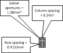
    5. So, you will want a aperture array of 2x3, with each aperture being 1.38mm square. Now, you want to figure out how to place them on the pad. For this, add up the two widths of the apertures, subtract that from the pad size, and then divide the result by three (since there will be "space" between the left side, the right side, and in between the two aperatures.

    [3.5 - (2 x 1.38)]/3 ≈ 0.2467 - so, you'll want to have ≈0.2467 between the edge of the pads and the aperatures and in between the two aperatures.

    6. You do the same thing with the height of the pad (5.5mm). In order to set the distance between the aperatures and the pad and between the aperatures, you repeat the process, except now you have three apertures to space out and not 2.

    [5.5 - (3 x 1.38)]/3  ≈ 0.4533

    Now your stencil aperture array should look like this:

    As mentioned, the customer will need to test whatever they decide to do to make sure there are no manufacturing issues.

    Cody

  • Thanks Cody,
     
    Can you please email me the pic?  It’s hard to see and resolution is poor so zooming out doesn’t help.
     
    Thanks again & regards,
    John Garrett
    TI - AFA
    Cell: 240 687-0350