This thread has been locked.

If you have a related question, please click the "Ask a related question" button in the top right corner. The newly created question will be automatically linked to this question.

TPA3255: Channel C & D load Instability problem

Part Number: TPA3255
Other Parts Discussed in Thread: TPA3251,

From 4 sample devices - running BTL mode - channels C and D, exhibit an instability when loaded - typical 4 - 8ohm. The internal AVDD reference seems to becomes unstable -  outputs pulse ever closer to clipping, even when signal is no where near clipping. When C & D are unloaded, Channels A & B work to specification - and into clipping without any problem. The instability occurs with 0.5V - 2V input signals, and at any PVDD Supply voltage from 30V - 51V. 

I changed the IC to the pin for pin lower power device: TPA3251 operated at PVDD @ 32V and the problem does not occur on this device! 

Have followed the component values and PCB layout as recommended in the device specifications..

Are you aware of any problems with the TPA3255 device that would cause this issue? 

  • Hi David,
    It would be helpful to have some more information in order to debug this problem.
    1. What are the part numbers for the LC filter you are using?
    2. Is there a schematic available for your application?
    I think this might help explain what we think is happening.
    Regards,
    Dan
  • Hi Dan,

    1) Using 1uF 450VDC Polypropolene capacitors : EPCOS B32671P4105K, and 10uH Toroid Inductors: Constructed on KS107-060A (27mm Diameter, 14mm Inside Diameter, 9mm thickness) Sendust Toroid, 14Turns 18 Gauge copper wire.

    2) Schematic is:TPA3255 Amplifier Schematic.pdf

  • Hi David,

    Thanks for sending the information! It looks like you’re using a custom inductor. My suspicion is the inductor is dropping below 5uH for higher currents.

    1. Do you have any information or test data on the inductor you are using?

    It would be great if we had an inductance vs current plot. Then we could ensure that the inductors you are using will keep the TPA3255 stable.

    It’s possible that there is enough variation on the inductors that the ones on channel A and B are sufficient and the ones on C and D are not if these are handmade. This would also explain why you were able to use the lower power TPA3251 without issue – you aren’t hitting the same current on the curve.

    Looking over the schematic everything looks good but I am a bit confused by the network after C14 (the one with L3, C8, R1, and C15). So my second question would be

    2. Can you explain that output network you have before CON1?

    Best regards,

    Dan
  • Hi Dan,
    Thanks for your speedy reply...
    The inductors are custom, unfortunately I don't have equipment that can determine inductance with DC bias as high as 13 Amps.
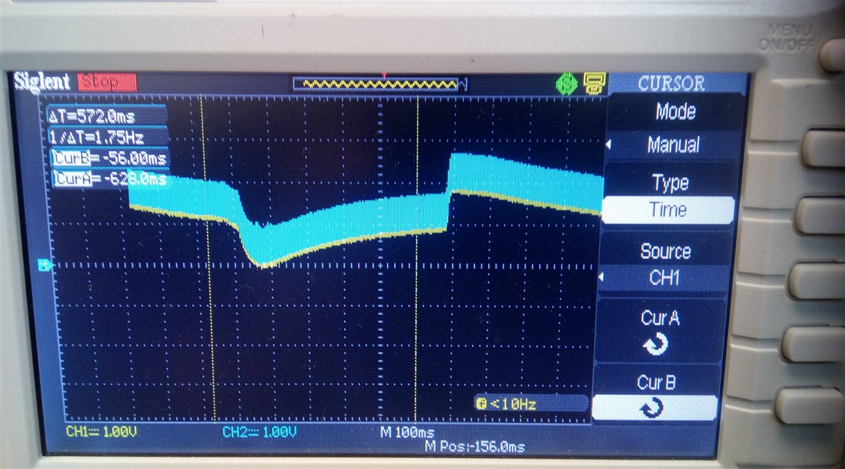
    However this instability problem begins at low currents, i.e, as low as 0.5A with 1KHz sinewave 0dBu signal applied. The OTW pin pulses during the instability, and the outputs have a DC bias applied, hunting positive then negative at approx 570ms - 600ms intervals.
    From the Sendust Toroid core specifications, have calculated the expected inductance with DC bias of 13A; it falls only 20% from 10µH to 8µH. So still well within the 5µH limit.
    Also have tried other inductor types including 22µH versions of the Sendust Toroid (19turns), gapped Ferrite drum core and Wurth WE-HCI 1890 inductors - all still exhibited the instability.
    Regarding the extra filtering - L3, 6, 8, 10, and C15, 22, 35, 47: These provide extra RFI filtering for frequencies above 10MHz. Have found these are necessary to achieve CE and FCC compliance of a digital amplifier product which intends to have multiple amplifier zones leads longer than 10m. The Ferrite beads have 0.04 ohm impedance at 100KHz, but 56ohm at 100MHz. The capacitors are 1nF 200V NPO 1206 ceramics.
    Note; with the inductors shorted - the instability is still present.
    Best Regards
    David
  • Thought some oscilloscope images of the instability may be useful, the signal level is actually 10V/div - had 10:1 selected on probes

    When I said it hunts positive and negative - this is about the Mid PVDD level.

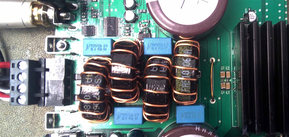
    One thing which is different to the TI PCB recommendation - is that the trace length to the inductors is not symmetrical - as I was trying to obtain a narrow footprint. See image of prototype.. Perhaps this may have some influence?

    Best Regards

    David

  • Hi David,
    Thanks for the information. The scope shots and layout are definitely useful.
    1. Could you send me the full layout?
    2. Can you explain the test that lead to the oscilloscope image that you sent? What is the input? What are the probes connected to?
    3. Is it possible for you to probe the PWM output? An oscilloscope capture of that would be useful.
    4. You mentioned in the first post that you have four samples. Do all of them exhibit this behavior?
    Best Regards,
    Dan
  • Hi Dan,

    The oscilloscope CH1 & CH2 probes were connected to the Left and Right +Ve Outputs at the 8 ohm load resistors. The output level was 10V pk - pk, with 0.3VRMS 1KHz sine-wave source applied. The oscilloscope time base was very slow to show the instability.  

    Yes all 4 TPA3255 samples from the TI sample store exhibit the same issue - on 3 identically assembled PCB's.

    I kludged the Output filters under the PCB so that they all had identical path lengths, and the capacitors all had excellent 0V bonding - instability still occurred - that rules out asymmetric track length from PWM pins to inductors. 

    I probed the PWM output - the C & D Channels  behave as expected - when entering clipping it sheds pulses. However more interestingly when I probe the Channel C input during the instability there is a bias variation which is the exact variation (with 21.5db of gain) I see on the amplifier output.  When I change this probe to 1:1  (1M input impedance) the instability becomes less prominent. 

    If I add 1M ohm resistor from each amplifier input to ground it becomes stable - but now clips asymmetrically - hitting the positive rail first with increased signal level.   So should I try also connecting 1M ohm resistors from each input to AVDD ? Will AVDD have suitable driving impedance - it is only effectively 250Kohm.  

    Best Regards

    David

  •   2X150W.pdfHi Dan,

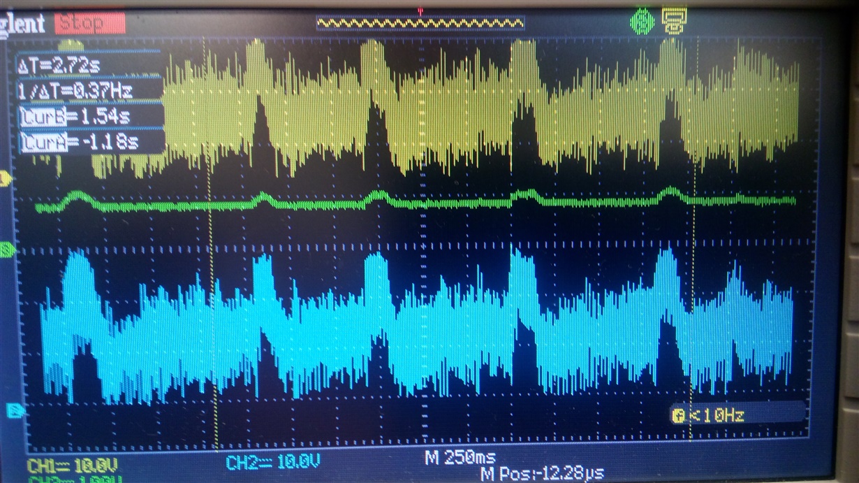
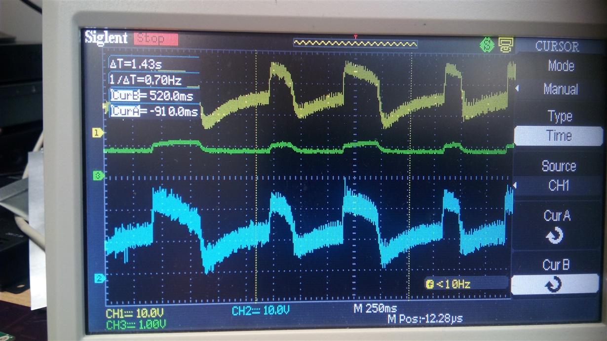
    Well - the instablity was only solved with steady state 1KHz sinewave source, as soon as I played regular program music the problem was back.. Somehow AVDD has DC bias glitches on the TDA3255 devices, while a TDA3251 device in the same board does not.

    The glitches occur at a rate of about 550 - 600ms.  If the AVDD capacitor is increased to say 4.7uF - it make no difference.  Have attached an oscilloscope image showing the AVDD glitches and how it effects the output bias. Have attached a couple of scope images showing glitches - AVDD REF Probe is CH3 (Green) while CH1 and CH2 are on the output Loads- See how they get large DC bias movements causing the outputs to go into clipping, when the level is clearly not large enough.

    Also added the PCB design since you requested it..

    Hope you can help solve this AVDD ref. problem.  The capacitor on this pin is the recommended 1µF 0603 X7R ceramic capacitor.  

    Regards

    David

  • Hey David,

    After reading through your tests, I'm wondering if we have investigated outputs of the op-amp input stage thoroughly. If there's any issues in the input, the amplifier will only make them louder. Could you verify we are getting a good clean signal at the output of the op-amps?

    The layout looks like it may also cause some issues. The ground trace wraps around the device causing very poor ground reference from the analog side of the amplifier to the power side. We need to watch out for ground voltage offsets across the substrate of the device.

    Regards,

    Dan
  • Hi Dan,

    The OP-AMP outputs are clean - the glitches do not appear on any of the 4 OP-AMP outputs. On the amplifier side of the 10µF electrolytic capacitors the DC bias glitches occur. The Electrolytics are general purpose Nichicon brand parts.

    Regarding the analog ground reference. I could try cutting the bottom layer ground plane. try and isolate the analog ground plane more from the power ground pane. Presently it is a very solid plane on the bottom layer.

    Regards

    David


  • OK I have cut the ground plane on the top and bottom layers so that there is only a connection between Analog and Power ground planes on the TOP layer directly below the TDA3255. The instability is still there - perhaps worse.

    I tried 47µF capacitors instead of the 10µF between op-amp outputs and TDA3255 inputs - it changes the glitch period so that it is typically 3.6s instead of 600ms.

    Regards
    David
  • Hi David,

    Could you try ceramic caps instead of electrolytic on the inputs?

    Also I see that C24 is 47uF on your schematic and we typically recommend 470uF for c_bulk on VDD.

    Regards,

    Dan

  • Hi Dan,
    Changed electro's to 22µF 1206 X7R ceramics - still has glitches.
    Changed C24 to 470µF - still has glitches.

    Regards
    David
  • Hi David,

    Thanks for trying those suggestions. I’m trying to gather as much information as possible to try to diagnose your issue. Could I get all of the layout files? We can exchange this information privately.

    Could I see waveforms for the input signal to your board, the output of the op amps, and after the capacitors of the op-amp outputs /TDA3255 inputs? I want to get an idea of where we can and cannot see these glitches.

    Regards,

    Dan

  • HI Dan,

    Do you have a viewer for Altium PCB files?  Am happy to send the files for the prototype board, how do we exchange this info privately?

    On the prototype board there is a  Coax and/or Toslink digital Audio - analog conversion, whose output I can feed through an external pot to analog inputs. The Analog inputs go to the buffer amplifier prior to the TPA3255.

    Will gather the required signals shortly.

    Regards

    David

  • Hi David,

    Yes we can view Altium PCB files. I've sent you a friend request which will allow us to take some conversation offline and share files.
    I look forward to seeing the signals!

    Regards,
    Dan
  • Hi David,

    I just wanted to put some details on the E2E in case anyone else has a similar issue and finds themselves on this post.

    After some more testing and reviewing the layout offline, we determined the layout was most likely what was causing the issue. Attached are some tips for layout on the TPA32xx family.

    Regards,

    DanTPA32xx Grounding Notes.pptx