This thread has been locked.

If you have a related question, please click the "Ask a related question" button in the top right corner. The newly created question will be automatically linked to this question.

INA225-Q1 leak voltage

Other Parts Discussed in Thread: INA225-Q1

Hi,

I want to ask about INA225-Q1.

Could you please confirm following question ?

* In case of inputting "Vs"=0V w/ "IN+/IN-" = 14.4V, is there possibility that the voltage which apply to IN+/IN- will sneak around to other terminals ?

I understood as long as input is 36V or less, it does not matter when Vs is at 0V.
However, we want to confirm that there is possibility that above thing will happen just in case.

Best Regards,

Machida

* In case of inputting "Vs"=0V w/ "IN+/IN-" = 14.4V, is there possibility that the voltage which apply to IN+/IN- will sneak around to other terminals ?
  • Hi Machida,

    As mentioned in the email, your understanding is correct. The supply voltage is independent of the common mode voltage. As long as you common mode voltage range stays 0V to 36V you should not see any problems. 

    Hope this helps! 

    Regards,

    Mayrim

  • Hi Machida,

    I discussed your question with my team and I will modify my reply.
    If your question is "having 14V on the inputs, will the output or other pins float to some unknown voltage?", then the answer is maybe. There are resistive paths all through the device that leakages could follow, it might not be a problem, but yes, there might be some motion on the pins when Vs=0v.

    Apologize I got the reply wrong earlier.

    Regards
  • Hi Mayrim-san,

    Thank you for your reply.
    I understand that there is no concern about device will receive damage when Vs=0V and having 14V on the inputs.
    If you can say even above, I have no problem at this time.

    Best regards,
    Machida
  • Hi Mayrim-san,

    Sorry for going back to previous this thread. However, We have addtional things which we want to know. so please continue this discussion.

    *Having 14.4V on the inputs(IN+/-) w/ Vs = 0V, what voltage will be observed on output or other pins ?
    * Also, is there possibility if other input pins have same conditon(Vs = 0V and having each input voltage),leakage path will appear as well ?

    It is necessary to answer these questions to get design win.
    So, I really need your help.

    Thanks in advance,
    Machida
  • Hi Machida,

    As I mentioned before, there are resistive paths all through the device that leakages could follow, there might be some motion on the pins when Vs=0v. This voltage at the output is unknown. It is not a regular operation of the device and I can't assure which voltage the customer will see at the output. If other inputs have same conditions leakage path could appear as well.

    Regards,
  • Hi Mayrim-san,

    Thank you for your reply.
    According to your comment, I guess that this device does NOT expect to be used applications which voltage is applied to input terminations(such as IN+/-) without Vs (means Vs=0V).

    Is my understanding correct ?

    Best Regards,
    Machida
  • Hi Mayrim-san,

    Could you please give me your comment ?

    Best Regards,

    Machida

  • Hi Machida,

    I believe that is what Mayrim is saying. This was not a scope intended by the designer, and therefore we do not have data to know what the voltage would be on those pins. 

    Carolus

  • Hi Carolus-san,

    Thank you for your response.

    Sorry, what I want you to confirm whether following understanding is correct or not.

    * I guess that this device(INA225-Q1) does NOT expect to be used applications which voltage is applied to input terminations(such as IN+/-) without Vs (means Vs=0V).

    The application like above, the leak current is also observed. Or depending on system, this leak voltage may impact to connected device.

    In above case(having certain voltage on the inputs w/ Vs=0V and want to prevent leak voltage to connected device), does customer need to care this voltage at system level ?

    I think that this question is a liitle bit nasty question, but I would like to give me a comment about above.

    Thanks in advance,
    Machida
  • Mayrim-san,

    Sorry for asking several times.
    But, let me confirm about below.

    * As I mentioned before, there are resistive paths all through the device that leakages could follow, there might be some motion on the pins when Vs=0v. This voltage at the output is unknown.

    You answered above for my question, but I think that leak voltage will be less than input voltage in following condition(IN+/- =14.4V) because the leakage path consists of resistive.

    * Vs = 0V , IN+/- = 14.4V and other inputs are 0V.

    Is my understanding correct (I understand that you can NOT answer exactly voltage value. But I think that voltage drop will happen by resistive path, so observed leakage voltage should be less than input voltage.)

    Best Regards,
    Machida
  • Hi Machida,

    This configuration is outside normal operating parameters, unfortunately the behavior is undefined. If your customer insist on using this configuration they will need to characterize the system to find out the average leakage voltage/current that could exists. I am sorry we can't help you with more data, I don't have it. This device have not been tested outside recommended specs.

    Regards,
  • Hi, Mayrim-san,

    Thank for your reply.

    How do you think for "Vs" pin and "GND" pin ?

    I understood that leakage path will appear at the I/O pins, however, I want to ask for "POWER" and "GND" pin.

    Do you think that leakage voltage will appear at "Vs" pin and "GND" pin as well ?

    Best Regards,

    Machida

  • Hi Machida-san,

    There are resistive paths through the silicon that could allow voltages to appear at floating nodes. I can not comment on specific pins, this is just an usual way to operate the device, I do not know what will be the behavior. 

    I apologize, I know you would need more information but this have not been tested and it can vary from device to device. 

    Regards

  • Hi Mayrim-san,

    Thank you for your reply.

    Understood..

    So, I would like you to discuss about schematic to avoid leak voltage.

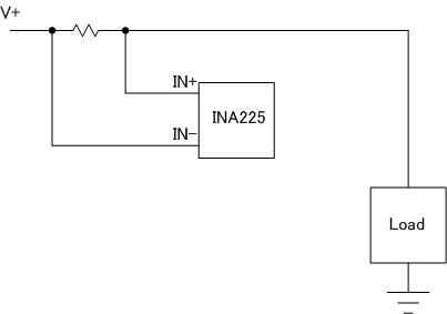
    We will use this device at high side(Please see following figure). To use high side switch is one of the idea to avoid leak voltage.

    However, it is a little bit expensive, so could you confirm that we can use the circuit to avoid leak voltage by discreate ?

    Best Regards,

    Machida

  • Hi Machida-san,

    I have a few questions:

    1. V+ in your schematic is Vcm (Common mode voltage)?

    2. Where exactly is the switch? I don't see it on the schematic. 

    Regards,

  • Hi Mayrim-san,

    Thank you for your reply.

    1. V+ in your schematic is Vcm (Common mode voltage)?

    Yes (Not differential).

    2. Where exactly is the switch? I don't see it on the schematic.

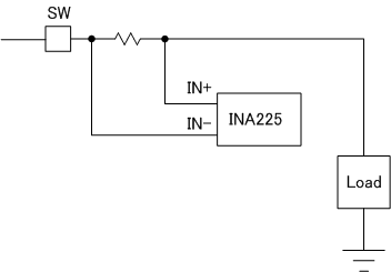
    Please see below. However, this is one of the way to avoid leak voltage. I want another way to realize this issue.

    Best Regards,

    Machida

  • HI Machida-san,

    If you connect a sw you will just disconnect the device from Vcm and if not Vs is applied the device is just off, nothing will happen. Of course no leakage because no power is applied to the device. I don't believe this is a good idea.

    At this moment I can't think of ways to avoid leakage voltage if Vcm is applied with Vs=0V. I will ask some colleagues to see if any idea comes up.

    Regards