This thread has been locked.

If you have a related question, please click the "Ask a related question" button in the top right corner. The newly created question will be automatically linked to this question.

INA240: Half TSSOP package Kelvin from via bottom PCB

Guru 54057 points
Part Number: INA240

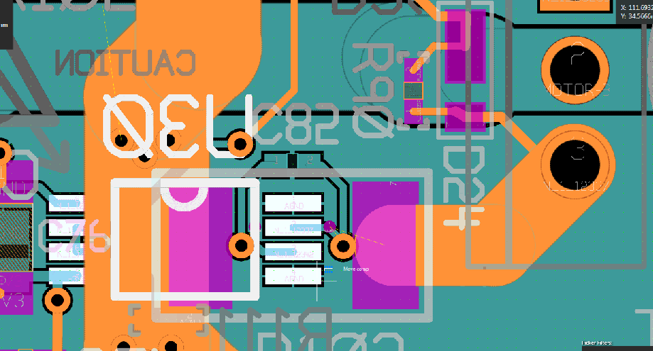
How is magnetic immunity of INA if placed half footprint pins-1-4 bottom of PCB yet centered under one shunt pad located on top PCB? So TSSOP package aligns center in only one of the shunt pads. It seems the long width of the TSSOP package was designed for tight layout situations described below.

Monitoring low side PWM where one half TSSOP package pins 5-8 may sometimes lie directly under the shunt ground feeds top side of 0.094" thick PCB.  

Very short leads roughly 0.5mm from shunt to pins-2,3 and require 1 via from Kelvin on each side of shunt pads similar to 11.2 layout example. 

Like this:

  • BP101,
    I don't think we have run any magnetic immunity tests for PCB component interference. I am getting some EMI testing done on the EVM though, but that may be more of a gross functionality report than a performance report.

    I recall that every via adds 11pH of inductance to the line. If the Vsense signal generated switching frequency is affected by that, I can't say. Usually we advise people to avoid vias for their kelvin connections but the bias current through those traces should be small enough that it's not too affected.

    Make sense, or am I missing your question's intent?
  • Hi Jason,

    Jason Bridgmon said:
    Make sense, or am I missing your question's intent?

    Partly answered via (11pH) and PCB design rules errors will not allow Kelvin trace from via into shunt pad from bottom, reason for edge of via connected to pad.

    Question is will EMI surges through the ground trace (orange) top side PCB effect the INA located bottom PCB (cyan). Other words does the INA bottom case have a shield to stop outside EMI or will EMI traversing the case even effect the INA performance? Seems to me the PCB ground plane creates an EMI shield of shorts since eddy currents in the copper under INA seemingly should buck the flux back into the analog ground bus.

  • BP101,

    I spoke with our design team about this and they said that there could be some interference as we left off the typical filtering cells we put on the inputs of the amplifier.  Filtering the inputs would work directly against the main benefit of the INA240, which is the high-speed common mode rejection.  There are no special EMI filters in the package itself, but I agree with you and sometimes I've used ground planes to isolate sensitive analog signals from high speed digital signals to avoid interference.

  • Hi Jason,

    Oddly never received an email message for your response on June 1.

    Jason Bridgmon said:
    as we left off the typical filtering cells we put on the inputs of the amplifier

    I was more referring to the case design EMI shielding. However still curious did the INA240 EVM package EMI testing reveal any facts about ambient EMI case tolerance, differential amplifier or output waveform interference?

    Thank you!

  • Hi BP101,

    Jason is not at his office for this week, I will ask him to review this upon his return.
  • BP101,

    The EMI testing of the INA240EVM was put on hold due to unforeseen circumstances, but resumed earlier this week. I hope to have something to share shortly!