This thread has been locked.

If you have a related question, please click the "Ask a related question" button in the top right corner. The newly created question will be automatically linked to this question.

High Side Current Sense-Clarifications Required

Other Parts Discussed in Thread: LPV811, OPA369, INA190, LPV821, TINA-TI, LPV812

Hi,

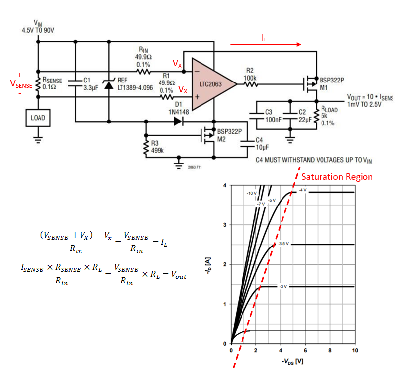
Please find the attached current sensing circuit.

It's output voltage equation is given by VOUT =( RLOAD *RSENSE* I SENSE)/RIN.

As per my knowledge the equation is derived as given below

Current flowing through RIN =(RSENSE*ISENSE)/RIN

The same current flow through RLOAD,multiplying this current with RLOAD will give Vout.

My confusion is to derive like as shown above voltage at the inverting pin should  be zero .As per my knowledge it is not zero in this case because

non-inverting terminal is not connected to ground.Please correct me if I am wrong.

May I know how the Equation of Output voltage is derived.

May I know the use of mosfet's M1,M2,D1 and Ref.

Regards

Hari

  • Hello Hari,

    Thanks for reaching out on the forum. So you can get the gain by setting the inputs to the LTC2063 amplifier to Vx. Thereupon, the upper node where Isense crosses Rsense has the voltage Vsense+Vx.   If you divide the difference between this node and the (-) input you get the IL current that passes through M1. The M1 transistor is operated in the saturation region so that it will drop whatever voltage necessary to maintain the drain current IL (I would look up regulated current sources if you need additional information on this). This current that passes through then creates the voltage across the RL resistor.  

    REF is used to keep the LTC2063 operating within device specifications, as the supply can only be 5.5V above the negative supply or ground. M2 provides the LTC2063 negative supply a means to float with the common mode voltage which can be anywhere between 4.5V and 90V. D1 helps with biasing M2.

    We actually have a similar circuit here and we show how to design for floating the device ground. Another thing to note, if you do not need such a common mode voltage, you might consider our INA190 (VCM<40V) and reduce your BOM count. Otherwise, possible TI substitutes for the LTC2063 include the LPV811, LPV821, and OPA369.


  • Hi Patrick,

    Thank you very much. I clearly understood the Vout derivation.
    May i know how we make sure that PMOS is in saturation region.Condition for PMOS to operate in saturation region is" |Vds|>|Vgs|-|Vth|"
    Here Vd is Vout Vs is Vx. I am confused regarding the Value of Vg. As per my understanding "=(V+ - V-)*Open loop gain of opamp". Please correct me if I am wrong.In this case what is the voltage coming to inverting and non inverting terminals of the opamp.May I know how the value of R2 is obtained as 100K .Please tell me how to check the M1 is in saturation region or not.

    Regards
    Hari
  • Hello Hari,

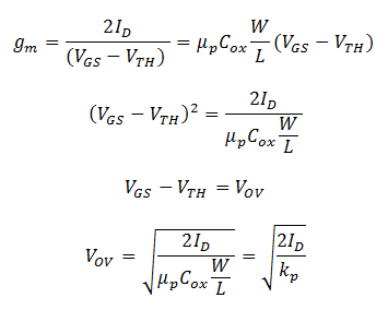
    To determine if your Vgs is within the saturation region, it may help to first derive the curve that separates the saturation region from the triode region. You can do this through two different methods.  The first is to calculate the overdrive voltage for a given drain current value.  The overdrive voltage (Vov) corresponds to point on the above said curve. The formula for Vov can be seen below. 


    Kp is known as the transconductance parameter and may or may not be found in the datasheet.  However, regardless of whether it is in the datasheet, it should be in the simulation model.  If it is not in the model, then it can be calculated from Uo and Cox, which should be in the model.  BSP322P has kp defined in the model.  However, it appears that Infineon defined it differently for certain conditions.  If you know which sub-model corresponds to your system conditions, you can pick the correct kp.  Otherwise, you may want to proceed with the alternative method.

    For method two, you can do some approximation to determine roughly what Vov would be.  We know that the general equation for a parabola is (x-h)^2=4p(y-k), where (h,k) corresponds to the vertex, which in this case is approximately at (0,0).  If we use the ID vs VDS curve in the datasheet we can approximate p, which for me was around 1.4.

    Once you have calculated a Vov for a given ID, I would then use the typical VTH value in the datasheet to get VGS.  You can verify through measurement if your VGS is around this value and confirm that the device is in saturation.  You could also take measurements while raising and lowering the common mode voltage to your amplifier to see that the current stays stable while VDS changes.

    The reason there is a 100k resistor is that the amplifier only has so much drive capability and the input capacitance of the BSP322P may make the amplifier unstable.

    For stability, the following must be satisfied: 

  • Hi Patrick ,

    Thank you very much for your time .

    I tried to do the DC analysis of this circuit to know more.

    If you dont mind I still need some clarifications.

    Attaching the DC analysis word doc so that you can review it easily and put your valuable comments

    Regards

    Hari

    DC ANALYSIS.docxDC ANALYSIS.pdf

  • Hi Patrick,

    Regarding pole frequency ,pole should be placed after 20K ,please correct me If I am wrong.
    If pole is placed inside the BW then circuit will oscillate ,correct me if I am wrong

    Regards
    Hari
  • Hello Hari,

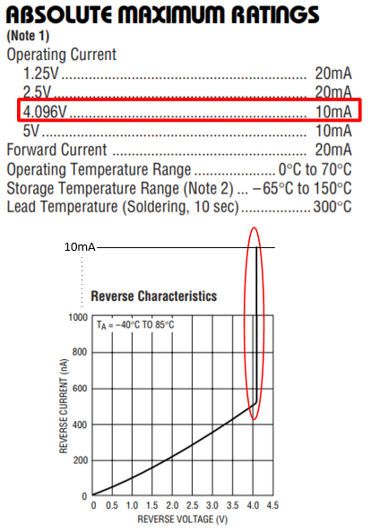
    I am not sure where you get 1uA for the REF. Based on the datasheet, it appears that REF can provide the proper voltage drop for reverse currents above 500nA up to 10mA (see figure below).

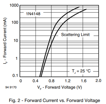
    For M2, the diode can have a forward voltage lower than 1V according to the figure below. Due to the quiescent current of the LTC2063, C4 will charge up to a voltage that is above ground such that |VGS|≥|VT| and most likely such that |VDS|>|VGS|-|VT|. The diode keeps the quiescent current from flowing across the 499K and also ensures that that VGS does exceed the gate source voltage specification in the datasheet.

    As for the resistor, I have been told that a general rule of thumb adding a resistor and lowering the pole frequency typically helps. However, upon looking at the open phase gain plot in LTC2063, it does look as though you could run into some issues if the pole is too low as you may have the phase reach -180 degrees before the gain reaches 0dB. In that case you would have a negative phase margin, and a negative gain margin. Keep in mind it takes about 3 decades for the phase to drop 90 degrees for a single pole, while the gain will only drop 20dB per decade. For a little more information on this, I would recommend the following link. Otherwise, I would refer to one of the analog books by Razavi, Sedra and Smith, or Gray and Hurst.

    Caps C3 and C2 I believe are outside of the loop and are meant for filtering the output. These can be calculated according to you RDS range and the minimum bandwidth you need to measure in your system.

  • Hi Patrick,

    I got the 1uA from the below spec in the datasheet of LT1389.

    Diode anode voltage is same as voltage drop across R3,but how to determine the cathode voltage because it is directly connected to Negative supply of OPAMP,

    May I know how Quiescent current charges C4 because negative terminal is not directly connected to any power supply.

    Is the Quiescent current is coming from the Positive supply.Please clarify

    Regards

    Hari

  • Hello,

    Tha 1 uA appears to account for device variation as some devices may have a minimum operating current as high as 1uA.  I presume any devices exceeding that specification are discarded and not shipped.  Otherwise the typical devices most likely have performance similar to the graph in my post above.

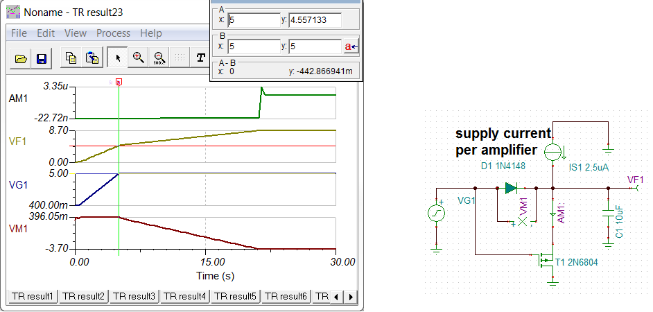
    For fast  changes in the common mode voltage  and the lower node of REF, the cathode will be a forward voltage drop across the 1N4148 as the 10uF will prevent the voltage from quickly changing on the cathode side of the IN4148.  Once the voltage across R3 is static. The cathode side voltage will continue to increase as the cap charges from the LTC2063 supply current.  Once the cap charges sufficiently high (|VS|=|VTH|), the MOSFET turns on.  The circuit I have below illustrates this.  In this case I used a 2N6804 which has a threshold voltage of about -3.7V.  

    The quiescent current (supply current) comes from the positive supply side and runs through the part.

  • Hi Peter,

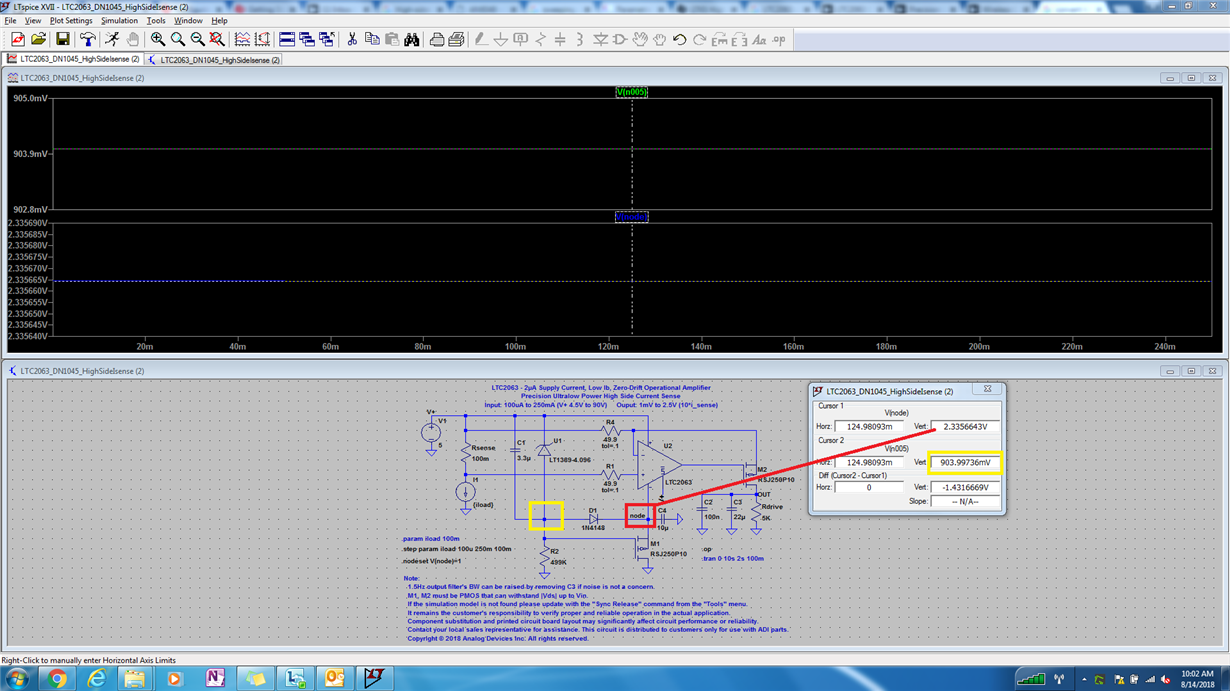
    Thank you very much.I tried to simulate the circuit, the voltage at the source of M1 is coming to be 2.3V. Please find the attached image, also sending

    the simulation files along with this mail.

    www.analog.com/.../LTC2063_DN1045_HighSideIsense.asc

    Regards

    Hari

  • Hello Hari,

    From your schematic, yellow - red= in my schematic VM1. The only reason .903-2.3 = -1.4V is different is because you have a MOSFET with a lower VTH (-1.4V) while my mosfet's VTH is -3.7V.
  • Hi Patrick,

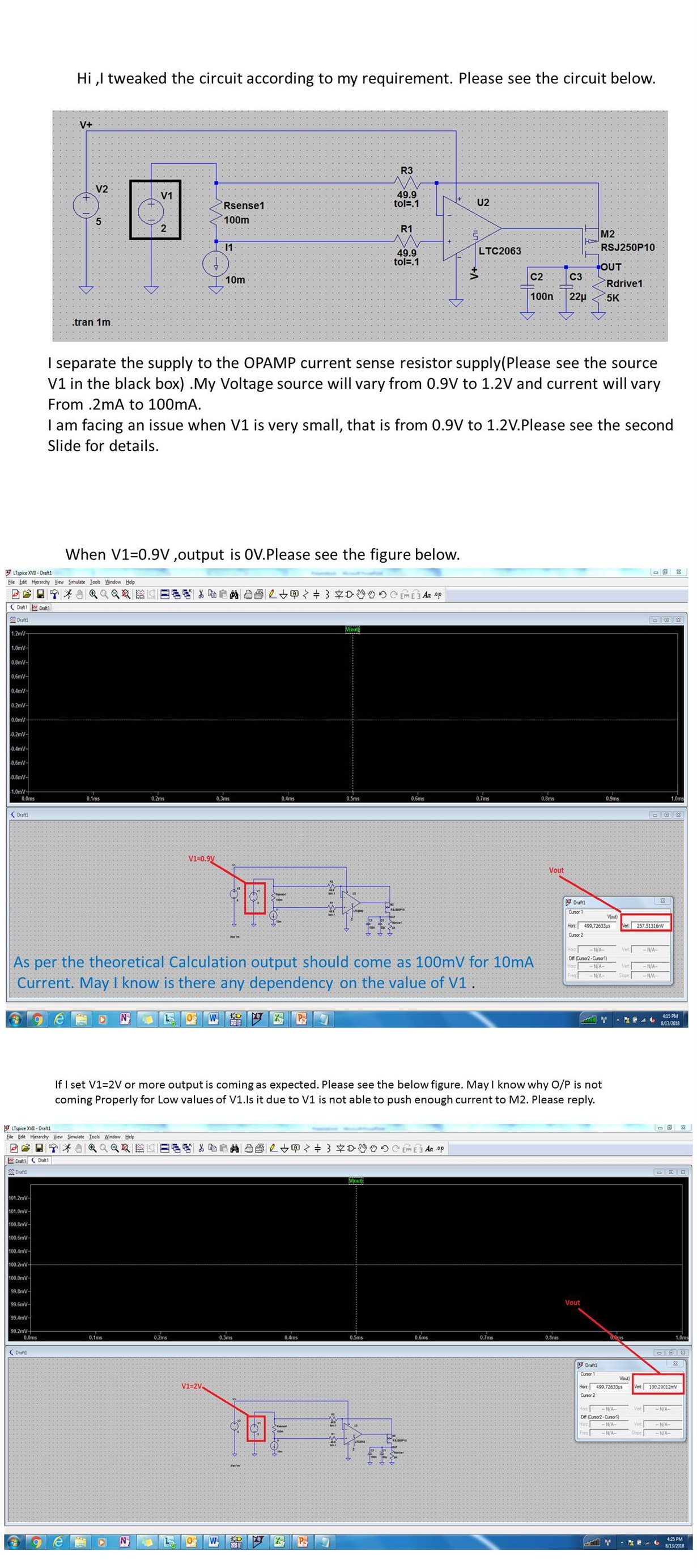
    I changed the above schematic according to our requirement.

    Separated opamp supply and current sense supply. For low values of current sense supply(V1), the o/p is not coming as calculated.

    Forst I put V1=0.9V and simulated the circuit,I got 0V.Proper O/P is coming only after I put V1=2

    Please see the figure below. If you don't mind could you please check the below circuit

  • Hello Hari,

    If I understand correctly, when V1 < 2V, your OUT=0V. This makes sense as the VGS of your RSJ250P10 is probably 3V or greater and it needs to be at between -1 and -2.5 to actually turn on. I am actually surprised it turns on at all with such a low source voltage. To properly turn on the p-channel mosfet to pass current, you must have a larger V1 (VS) for this kind of layout.

    If you have further questions, I will pass the along to our op-amp group. They can most likely give you a similar solution with TI parts and thereby provide some more meaningful support for you. Also I would like to inform you of an alternative spice platform called TINA by DesignSoft. That is typically what we use.
  • Hi Patrick,

    Thank you very much ,I will change the MOSFET and see,will make a circuit in TINA using the equivalent of LTC2063 suggested by you.
    If the circuit is not working with new mosfet then definitely post in TI's opamp forum

    Regards
    Hari
  • Hello Hari,

    Have not heard from you in a while. Not sure if you were able to get a circuit together that fits needs. Please let me know below if you still need help on this and I will reach out to our op amp team if necessary. Otherwise, I am closing this thread.
  • Hi Patrick ,

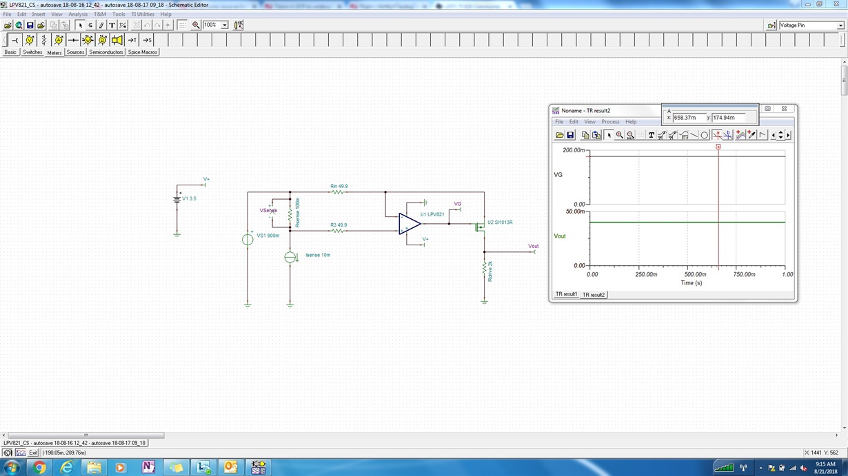
    Sorry for the delay .I made a circuit as shown above using TI IC's

    Please find the attached.Could you please mathematically show how 174mV is coming at gate of MOSFET

    Regards

    Hari

  • Hello Hari,

    I actually made a mistake in my last post. As the negative input is oriented at a higher potential than the positive input, the output of the op amp and Vg to the mosfet will actually go low. As the drain voltage would still be so low, I believe you will still not exceed the threshold voltage to turn on the MOSFET. On that note, I noticed in your above TINA test you decided to replace the PMOS with an NMOS in which it's source is oriented above the the gate. I do not think this will work for you. If you proceed with using the NMOS, I would re-orient it such that the drain is on top and I would swap the inputs for the IN+ and IN- of your op amp.

    The op-amp output I would expect to rail out at a little above ground or a little below supply depending on how the inputs are oriented. For how close the output will move towards to the rail limits, an op-amp team member may be able to give you a method to calculate. As such I am passing this thread along to them.
  • Hello Hari T,

    Perhaps you are expecting circuit designed for 4.5-90v to detect shunt CMV below 4.5v? Notice the 100uA low sense was likely only detected as Vin nears 4.5v.

    Hari T O0 said:
    Forst I put V1=0.9V and simulated the circuit,I got 0V.Proper O/P is coming only after I put V1=2

    Perhaps you need to increase OP input bias just above minimum device specification, at risk of Max Vin (90v) destroying OP in exceeding maximum datasheet input bias spec. 

    Seemingly as Patrick mentions M2 will saturate DS as the gate drive nears Gth, e.g. not returning to GND. If the shunt signal is pulsing M2 gate will likely have some aspect of the original monitored signal. Thus the circuit as you come to understand must be modified to fit your application (V1=0.9v) for sense current across CMV being below 4.5v input voltage. Perhaps M2 saturation more tricky under pulsing gate drive, though 22uf should set RC time constant well above M2 pulse off time.

  • Hi BP and Peter,

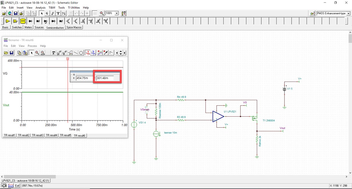
    I changed NMOS to PMOS as Peter suggested.Now at mosfet gate I am getting a voltage of 300mV.Could you please mathematically shows (with the help of equations) how that value is obtained at gate of MOSFET.

    My output voltage is coming as per my calculations.But I am not able to find the gate voltage(O/P of OPAMP).Please help me to find it out.

    Regards

    Hari

    LPV821_CS - autosave 18-08-16 12_42 (1).TSC

  • Hari T O0 said:
    I changed NMOS to PMOS as Peter suggested

    Was it not always a PCHAN in the circuit? Hard to see the arrow in last few of your grey looking analysis arrow is blurry. 

    Hari T O0 said:
    Now at mosfet gate I am getting a voltage of 300mV.Could you please mathematically shows (with the help of equations) how that value is obtained at gate of MOSFET

    It would seem analysis ignores specific gate threshold voltage required well above 400mv. Perhaps due to analysis with out floating DC supply OP? That likely being some part of the original circuit not being present in Tina circuit? Not to forget OP input bias perhaps restricted to the original intention for circuit operation from a minimum (+4.5v) up to maximum (90v). Have you not changed the circuit operation points and not reduced values around new point (shunt R or E=IR) to include new reduced CMV minimum? Check OP datasheet for input bias versus swing to rail graph, if one exist.

    Where is  VSense plot of CMV across shunt? perhaps use Vmeter. Well anyway the OP input bias output swing to rail is critical in your analysis.

    Who is Peter?

  • Hi BP,

    Instead of Patrick I wrote Peter,it was a typo sorry.

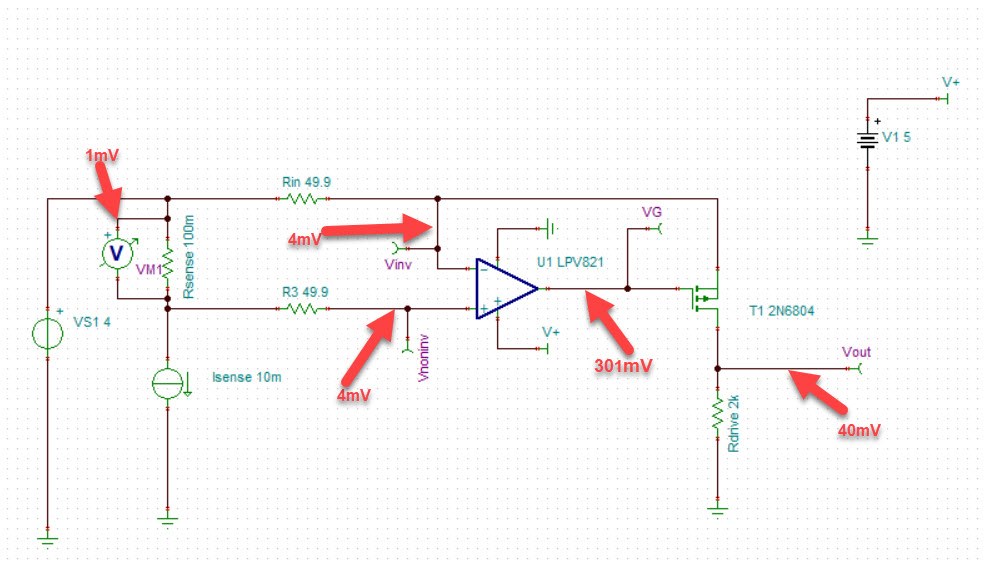
    Please see the attached image.

    You can see that 4mV is coming in the inverting and non inverting input of the opamp.

    As per my knowledge opamp will multiply the difference between inputs with its gain.Here both the inputs are same then how I am getting

    301mv at the op amp output.Is it due to offset voltage.This is confusing me.

    Regards

    Hari

  • Hari T O0 said:
    Here both the inputs are same then how I am getting 301mv at the op amp output.Is it due to offset voltage.This is confusing me.

    Perhaps from gate leakage, most likely suspect. Simply remove OP and gate plots VG relative to VS1=4v through T1 leakage 2k ground. Agree no differential input of OP the output only produce minimum leakage show shown in datasheet, 301mv seems bit high to be OP leakage alone.

    BTW: Try to run TA from operating point instead of initial conditions.

  • Hi Hari,

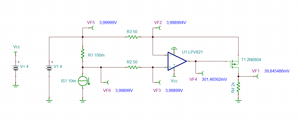
    U1 senses VF6 at the +input and adjusts its output voltage until the voltage at the -input equals the voltage at the +input. As result, a current of (VF5 - VF6) / R3 is flowing through T1 and (because now gate current is flowing) finally through R4. To make T1 this drain source current flowing, the output of U1 must generate the gate source turn-on voltage of T1, which is VF4 - VF2. So, everything is working as expected.

    Kai

  • Hi Kai,

    Thank you very much.
    If I divide VF4 by the difference of (VF3-VF2) will I obtain the Openloop gain of U1.

    Regards
    Hari
  • Hi Hari,

    don't forget the input offset voltage and the common mode rejection ratio of the LPV821.

    Kai
  • Hi Kai,

    I didn't get you.
    If you don't mind could you please elaborate your above statement.

    Regards
    Hari
  • Hi Kai ,

    Need one more clarification,may I know how you how you obtained VF2=3.998994V and VF2=3.99899V.
    When I am simulating I am getting only 4mv at both inputs.
    Do I need to change any settings in TINA-TI.Please help

    Regards
    Hari T O
  • Hi Hari,

    the TINA-TI DC analysis shows VF2 = 3.998994V and VF3 = 3.99899V. VF2 - VF3 = 4µV.

    This error voltage is the sum of the finite CMRR, the input offset voltage and the open loop gain of LPV812. Have a look at this very simplified calculation:

    The CMRR of LPV812 is 125dB. This results in an error referred to input of 4V / 125dB = 2.2µV. About 1.5µV of the 4µV comes from the typical input offset voltage of LPV812. And, finally, 4µV - 2.2µV - 1.5µV = 0.3µV is caused by the finite open loop gain of LPV812, which calculates to 301mV / 0.3µV = 120dB.

    Kai
  • Hi kai,

    DC analysis show only slight offset at differential inputs so how can OP output be 301mv? Other words with such little input offset 1mv DC error of CMRR (rejection to input noise) the output seemingly would be near zero volts at zero hertz, not 301mv. Something seems off in idea 120db rejection to noise 1Hz our output should be quiet as church mouse, right?
  • Hari
    It appears that you have been working on the same application in multiple E2E posts.
    if you have any further questions regarding the use of our low power amplifiers in this application, please feel free to open a new thread.
    Thanks
    Chuck
  • Hi Chuck ,
    Sure I will open a new thred whenever necessary.
    @Kai....Thank you very much for your time and concern.
    Regards
    Hari