This thread has been locked.

If you have a related question, please click the "Ask a related question" button in the top right corner. The newly created question will be automatically linked to this question.

INA240: How to work around input bias

Guru 54057 points
Part Number: INA240
Other Parts Discussed in Thread: UCC27714,

Seemingly low side monitor of idle inverter leakage current prior to PWM being applied might be pre-biasing the already internally biased INA amplifier.

Data sheet show VOS=5uv typical (IB) bias 90ua typical (IB+/- Vsence=0mv) yet typical inverter idle INA output noise when driven from UCC27714 gate drivers nears 680mv @20mv leakage across any low side shunt. Lower resistance value shunts do not seem to lower proportionately the internal pre bias from over driving INA output when PWM actually initiates real time inverter current flow. REF1=GND, REF2=+1.225v

Seemingly in series phase monitor would not have the same impact from low side NFET leakage current at higher inverter DC potentials nearing or exceeding VCM. Seemingly in phase monitor idle CMMV measured across a shunt would be far less and not impact INA internal bias circuit as does low side monitoring where inverter bias is always present prior to each and every PWM cycle. Does it not seem possible INA pre biasing the input of the PWM rejection circuit can produce excessive output measure overshoot when placed as low side current monitors?

Idle mode leakage across shunt, INA output signal inverter via clean linear 80V source filtered 28000uf DC. The INA feeds from 3v3 LDO after 5v buck switcher via isolated linear 24vdc.

  • Hello BP101,

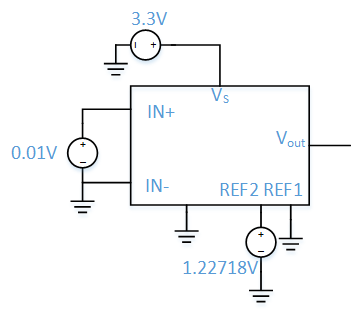
    I am looking into your issue.  I will consult our design team tomorrow to see if there is any condition in which they would expect the input bias to cause the errors you are experiencing.  However at this point I am concerned about the performance of your current device.  I would expect that if your device has REF2=1.225V, REF1=GND, and your VSense= 10mV (max positive peak), then I would expect an output of 1.225V/2+.01V*20V/V = 0.8125V.  I actually get pretty close to that value in my test setup shown below.

  • Hi Patrick,

    That's a fairly clean wave form used at INA input 10mv leakage current gets added into the answer.  Even Tina analysis extensive output filtering (470k/15n) produces an odd answer 40mv for IG1=8 amps, either way REF is configured. You really need to test INA input with a true motor PWM inverter to see this outcome. Tina Function generator sweep mode (ARB 39ms) around 12.5Khz PWM is not exactly simulating effect of trapezoidal wave crossing shunt IG1=8amps. Yet oddly a remnant of  trapezoidal wave form ghost appears with >30ms transient analysis.

    Seemingly pre-bias causes an ADC scaling issue ( VS=3v3) shunt leakage current somehow infects overall accuracy. It's almost impossible to snub out that added potential which changes the ADC full scale factor in bad way. It seems very aggressive 470k/15n series resistance on the output to get narrow signal slope from ADC samples. Yet even that would produce incorrect current measures judging from results so far.

  • Patrick Simmons said:
    I would expect that if your device has REF2=1.225V, REF1=GND, and your VSense= 10mV (max positive peak),

    Our test shunt 500uohm. Tina INA output produces 40mV/A peak @75 amps. Oddly 24vdc switching DC supply when powering test bench inverter, shunts get extremely noisy easily top 75-100mv 8-20mV peaks yet somehow the ADC 3k9/15n filter snubs those peaks. 

    Rechecked 100 amp bar inside 80v DC linear supply 750uohm (75mv@100amps), ground side same as the three INA's. The 500uohm shunts (6watt) derate roughly to 3 watt @100*C.

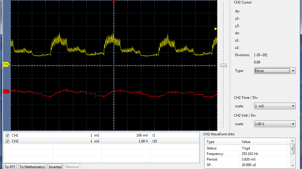
  • Updated capture of shunt CH1, INA output CH2, 8 amps test bench, REF2=GND, REF1=1.225v. Notice output peaks near same as when REF1+2=+1.225v or mid REF +1.225v series 9K1/6K8 to ground, roughly 680mv output bias.

    Bottom half of signal (CH2) closely qualifies for balanced PWM negative inverter current wave form. Note CH1 X1 probe was not showing the correct shunt signal.

  • Hello BP101,

    Please clarify your inquiry here by drawing what you would expect as an output from the INA240 overlapping the yellow output curve of the INA240.  I believe you are showing us that as the output of the INA240 approaches the REF voltage level, the noise increases.  I would expect that the output of the INA240 is increasing because something else in the system is sourcing more current through the shunt.  Please isolate the INA240 from the signal source and simply apply an input sense voltage to the INA240.  If, by isolating the inputs and providing a voltage, you still see the noise on the output, then we can rule out the source.  The next debug steps would be to isolate the output from the rest of the circuit and see if the supplied voltage creates noise, and finally to try sourcing the VREF directly with a lab source.  Once we identify the source of the peaking, we can target our debug efforts further.

  • Hi Patrick,

    The excessive peak noise across shunt was measurement error of the scope probe being X1 where X10 reduced noise more respectively 9-16mv peak.

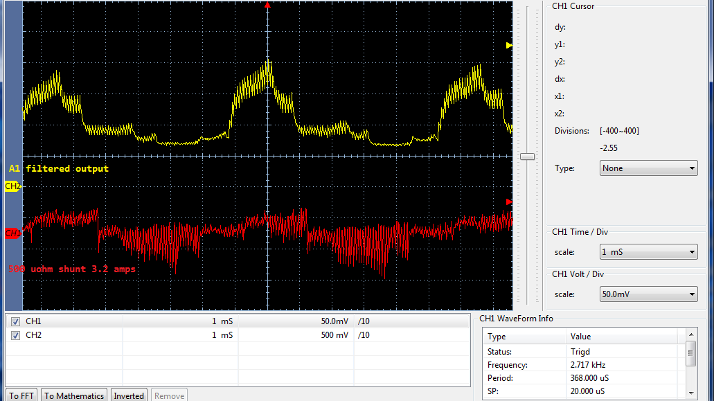
    Yet that is not explaining why 1/2 REF has no ability to reduce the peak magnitude of the A1 output during random transients and typical PWM peaks crossing the shunt. That is to say any shunt transient that reaches A1/A2 output exceeds the REF pins ability to constrain them being the transients attempt to reach VS pin 3v3 rail voltage. There seems to be scaling error in the output relative to VS 3v3 supply voltage and the 500uohm shunt should be creating under this current measure condition. There is no reason why ST current monitor 750uohm shunt 100 amp bar (75mv/A) can easily measure same low side PWM below capture but the 240 low side 10mv/A with SAR can not!

    Notice the shunt millivolts above capture  X1 probe and later with X10 below capture a true shunt signal is more revealing to how even 1/2 REF (620mv) output signal amplitude for 3.2-3.6 amps has excessive amplitude.  The amount of error is easily 30% no matter what the datasheet formula suggests. Below capture CH2 we see 2v peak - 1/2 REF (620mv) = 1.38v/10mv or 13.8 amp peak. The A1 output peak should be 10mv + 1/2 REF and 635mv/10mv/A or 3.5amps so the output has excessive unfounded magnitude! The INA output is violating Ohms law E=IR * 20 gain. Something in the INA use (not of our doing) is causing excessive gain A1/A2 which violates Ohms law as 12.5kHz PWM signal CMMV crosses the 500uohm shunt. That is in our opinion for TI lab technicians to figure out, not the customer to fall victim too. 

  • Patrick Simmons said:
    The next debug steps would be to isolate the output from the rest of the circuit and see if the supplied voltage creates noise, and finally to try sourcing the VREF directly with a lab source.  Once we identify the source of the peaking, we can target our debug efforts further.

    Our opinion differs as the INA240 should have been tested by TI lab to properly function as a low side monitor with 12.5kHz PWM present on the shunt. That is to suggest it was not judging from the results being revealed from two different DC inverters we tested it as low side monitor. Both inverters have proved the output amplitude must be resistively divided for the 240 to produce usable signal and SAR to have properly scaled ratio metric 3.1v full scale samples and measures.

    It is possible to provide TI lab bare PCB inverter to test why or how the 240 used low side monitor (12.5kHz PWM) the A1/A2 output violates Ohms law E=IR * 20 or 50 gain as it relates to REF, VS pins 3v3 dc supply. Perhaps it would behoove TI engineers to think outside the box sometimes.


  • Patrick Simmons said:
    If, by isolating the inputs and providing a voltage, you still see the noise on the output, then we can rule out the source

    The source is all the PWM input artifacts crossing the shunt and distorting the amplified signal thus leading to incorrect results. It dawns on me we have not considered certain PWM artifacts such as Delta V flyback to distort the amplified output scale. It is plausible the method of REF splitting under certain CMMV conditions may lead to device errata.

    What you are not directly aware (captures) are wild flyback pulse cycles INA is amplifying going above VS and below GND. Hence the MMZ102C ferrite on the output clamps down on some of the more destructive peaks. Again the 75K, 470k output A1 signal (isolation barrier to SAR) shows how the output impedance directly causes the differential gain to swing wildly upward just under VS rail.  You didn't see 30mv spike in the center (yellow circle shunt) also caught during a few single triggers. E.G. There is limited to no input CMM isolation of low side Delta V/T from effecting 240 output current gain, REF set output to mid supply or 1/2 precision reference. That's the nitty gritty and directly effects A1/A2 output settling time!

    New post to follow A1 handling of inductive PWM flyback pulses!