This thread has been locked.

If you have a related question, please click the "Ask a related question" button in the top right corner. The newly created question will be automatically linked to this question.

INA240: Initial large transient

Guru 54087 points
Part Number: INA240
Other Parts Discussed in Thread: UCC27714, TIDA-00909, INA282

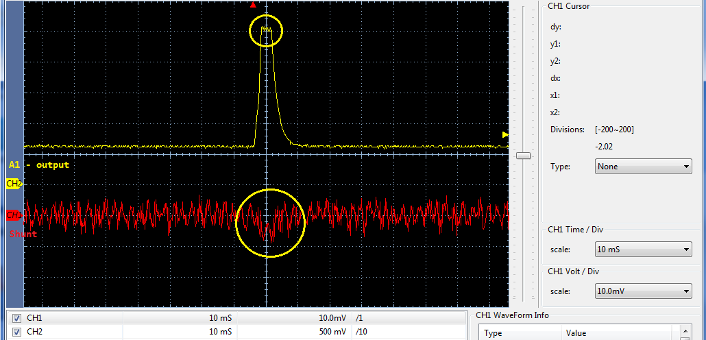
After making 75k series resistance output of A1 to SAR input a much larger transient occur to cause fault comparator trip. With 4R87k A1 output 1st transient pulse be just under comparator fault trip 2.7v. Below transient being far to large either way, A1 output has sudden gain explosion for no good reason we can easily pinpoint. The spike below would be 60 amps, no way has a 60 amp surge occurred!

Notice shunt signal lowers below ground yet A1 output seemingly moves in opposite direction, sometimes single 30mv pulse occurs. It seems the A1 must have much larger series R to stop sudden 1st transient. There is No 10k pull down on A1 output, seemingly may cause precision error % to increase? Otherwise wise 10k pull down on output would make path for ground noise to enter ADC channel.

Does the A1 output need much greater series resistance to stop current fold back effecting output? Does the A1 output specifically require a pull down R in order to normalize shunt inrush current from effecting the output gain magnitude in transient states?


  • A1 output 470k series resistor into SAR has even higher initial peak. Tina A1 model transient analysis produces plot with the inverse signal roll off of the bench model. Oddly AINx input (CH2) above should have 30ms rise time versus 5ms. Yet the A1 1st transient current pulse is greatly exaggerated immediately tripping fault comparator. This test seems to proves the A1 is directly causing unexpected comparator faults to occur.    

  • Hello BP101,

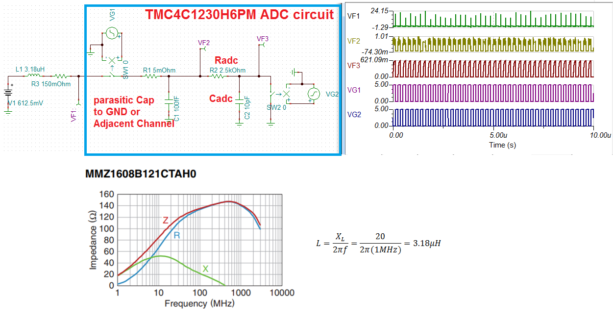
    Although our TINA models are not perfect, I think there are additional details you are omitting in your simulation.  From what I know, you do not include the ADC on your output in your system simulation model.  The ADC is not a passive device. It has switching elements in it along with input resistance and capacitance.  This is further complicated by the fact that it is a multi-channel ADC. From my understanding of your system, you have a large inductor (ferrite bead) in front of the ADC, which is probably inducing some of the peaks you are seeing.  Below I illustrate the point with a circuit that I believe closely emulates the actual front end operation of the ADC.  Below I also calculate the inductance of your ferrite bead.

    Based off of this, I think you should remove your ferrite bead and remeasure the INA240 output.  I also would isolate the output for at least one measurement to verify there is not any other other unexplained transients occurring on the output of the INA240.

  • Hi Patrick,

    The ferrite bead MMZ102C (1k imped) clamps high frequency ringing + transient peaks as all ferrites do but only at certain frequency does the impedance increase. Actually stops a lot of PWM ringing other trash from entering ADC plus we add 3v3 TVS diodes before the ferrites. Those ferrites actually stopped false tripping of the comparator during run time but the bigger problem is the added running amplitude nearing 2.7v is not correct at all.

    Yet far off from what is occurring in the test bench captures posted above as a spike on the shunt is directly driving a transient peak amplitude near 2.7v on the A1 output. The bigger problem is the low level shunt noise, roughly 20mv  (9-16mv X10 probe) is not being filtered by the PWM rejection circuit and gets incorrectly added into the output as measured current.

    The only resolve is to improperly resistively divide the A1 output or add excessive input filtering. Such being done in other uses of the A1 TIDA engineers for noisy shunt conditions. That is counter intuitive to the datasheet explanation warning us to not add external filters on the input, the output should not require heavy filtering either. Yet in reality the datasheet fluff written PWM rejection transient suppression is a false narrative under low side monitoring!

  • Patrick Simmons said:
    Based off of this, I think you should remove your ferrite bead and remeasure the INA240 output.  I also would isolate the output for at least one measurement to verify there is not any other other unexplained transients occurring on the output of the INA240

    Great idea yet the transient above capture/s stops any motor run very first pulse. That 2.7v peak lowers when we drop A1 output amplitude with 4.87k, motor runs ok. Again the 20mv shunt noises added into A1 output magnitude very troubling, as it should subtract or reject CMM noise -93db via  PWM rejection filter. Tina spectrum analyzer also confirms spectral power analysis of SAR input -93db @12.5Khz and comparator input over -190db down. Oddly there is a slight tweak up @12.5Khz but trace continues down to 400Kz after.

    Obviously TI engineering did not do an extensive study to include conditions where input PWM noise rejection might cause more mayhem than good.  Very plain to see we need more input filtering and limited output filtering and to determine how UCC27714 is seemingly gaining up idle shunt noise to 20mv (9-16mv x10 probe) Perhaps a winning focus to first get that shunt noise under control?

  • Hi Patrick,

    Removed the MMZ120C ferrites from A1 outputs, used 400nf (48mohm) multi layer chokes and made things much worse tripping fault at very low motor RPM. After that tested 525 ohm to ground after 3K9 on A1 output lowering signal floor to 310mv. Again A1 output peaks 2.7v during motor run easily tripping fault comparator, mostly from last 2 phases. No matter what REF or output bias level is made the output transient pulse magnitude is always excessive, both A1 & A2.

    Second review of idle shunt noise is 8-12mv not 20mv earlier detected. Seemingly after lowering the A1 output 4K87 to 3K9 the shunt noise reduced by half, with MMZ installed or without, 8-12mv of shunt noise is always present. That can't be good any noise above 5000uV/A since the A1 idle output becomes just as noisy in the 20V/V gain.
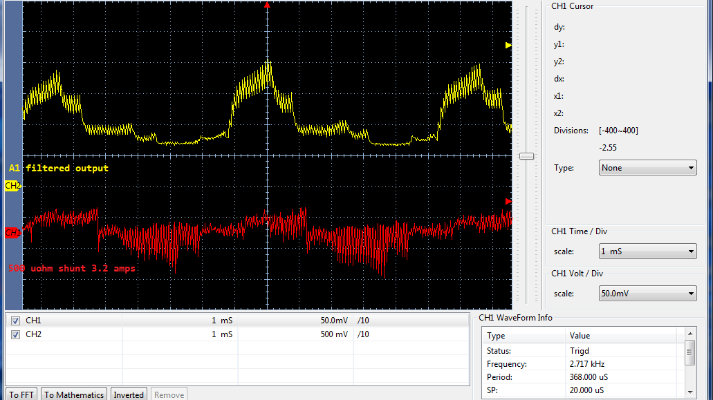
  • The shunt scope probe X1 10mv vertical was not capturing the correct signal above captures but X10 50mv is lowest vertical scale. Yet it seems the A1 input requires some filtering judging from the shunt signal. Capture below seems to explain why the A1/A2 are gaining up the reading, shunt signal is very transient 80us periods.

    The PWM rejection is not filtering random transients or EMI from entering the output signal, full blown input filter might better do job. Why the datasheet misleads anyone to believe filtering on A1 output can correct shunt signal issue is nuts. This shunt signal has to much magnitude from harmonics, the A1/A2 do not filter that high frequency part from entering the output. Hence MMZ120C ferrites are required on the A1 outputs and even that is not enough filter action to correct the error % the shunt PWM signal seems to create. 

  • Hello BP101,

    Thank you for your feedback.  To clarify a bit - the INA240 data sheet (section 9.1.1) suggests not using input filters in in-line applications where large voltage steps are going to be measured because they defeat the purpose of the PWM rejection circuitry and that the user to use their judgement as to what filtering to include.  Including the footprints for filters, both on the inputs and output, even if they are not used, is good practice as it allows for easy debug and can be bypassed with 0 ohm resistors and by depopulating capacitors.

  • That statement leads any reader to believe adding input filtering under any circumstance the INA will produce incorrect measurements from the added error. The same statement infers adequate PWM rejection filtering has been built into the INA device. Therefore it is not necessary to add filtering at all as most INA series illustrations inside application PDF too indicate. Why would anyone want to add error into the PWM transient rejection circuit. Fact is the 240 is passing more transients than 282 with a 50Khz switched capacitor filter. TI lab testing has fall short in this explanation as it relates to other family INA devices actually stopping most shunt transient with no input filter what so ever. We tested both devices against each other and the 282 wins hands down, how can that be?

    Several illustrations TI marketing PDF produce a false narrative to the reader that TI current monitors can compete with other devices on the market that also require no input filtering what so ever!

    And again several questions being asked are not being answered:

    1. Why the output is passing shunt transients when PWM rejection is supposed to reduce or even stop transients from reaching the output?
    2. Why does the REF pin level not reduce output peak magnitude proportionately in said transients reaching the output?
    3. Why is a 500uohm shunt producing incorrect A1 output level relative to 500uV/A being a true current measure?
    4. How can the 500uohm shunt CMMV (shunt capture) be so far from producing a correct transient response with PWM rejection on the input?
    5. The shunt seems to somehow be biased or driven by the INA input PWM rejection stage adding to the CMM magnitude. How can that be reduced and why is it not disclosed in datasheet such condition might occur under certain placements of the product?
    6. What is a work around to reduce shunt CMMV to match the INA internal PWM rejection circuit? Perhaps certain type mohm/A shunt materials are not compatible with PWM rejection?

    Difficult questions that comparison testing with real world PWM would have indicated. Perhaps harder questions in precision current measurements require common use lab testing procedures be put in place so TI customers are not subjected to questionable contradicting vague and non LAB verified quotes in datasheets!

  • Patrick Simmons said:
    Including the footprints for filters, both on the inputs and output, even if they are not used, is good practice as it allows for easy debug and can be bypassed with 0 ohm resistors and by depopulating capacitors.

    The datasheet recommened layout figure 39 shows no filtering components being added to the input. Contradicting the facts of a datasheet by adding unfounded opinion is considered by law being after the fact! If the INA device is failing to live up to the claimed statements the department must produce an errata document so customers are updated to later lab findings surrounding an integrated circuit relative to specific uses and purposes.

    Patrick Simmons said:
    suggests not using input filters in in-line applications where large voltage steps are going to be measured because they defeat the purpose of the PWM rejection circuitry and that the user to use their judgement as to what filtering to include.  I

    Also a contradiction of the stated datasheet facts, PWM rejection ability without providing an example of what would constitute special care where other INA devices do not require any input filtering to stop similar transients from effecting the output magnitude set by REF. The REF pins have no direct control over the A1/A2 output magnitude in side the transient response from/of input transients

    9.1.1 Input Filtering

    NOTE

    Input filters are not required for accurate measurements using the INA240, and use of filters in this location is not recommended. If filter components are used on the input of the amplifier, follow the guidelines in this section to minimize the effects on performance.

    Based strictly on user design requirements, external filtering of the current signal may be desired. The initial location that can be considered for the filter is at the output of the current amplifier. Although placing the filter at the output satisfies the filtering requirements, this location changes the low output impedance measured by any circuitry connected to the output voltage pin. The other location for filter placement is at the current amplifier input pins. This location satisfies the filtering requirement also, however the components must be carefully.

    Our design requirements called for no additional error being added by input filters. Lack of filtering is not causing the issue in the above statement of suspected errata. There is some kind of design issue/s with PWM rejection circuitry as it relates to low side monitoring of shunt bound PWM near 12.5kHz, the PWM frequency crossing the shunt. Again Tina spectrum analyzer reveals an upward spike in power level after 10kHz very near 12.5kHz. That spike is very odd and seems to relate to the issues being reported several times.

  • Hi Patrick,

    It would seem 10uh multilayer cokes produced better results than 200nH choke yet each allows Delta V/t transients to trip the fault comparator. The MMZ102C ferrite stops A1 output transients passed via both chokes we tested and perhaps the change in impedance to counter repeating transient cycles has a slight effect to increase signal pulses peak magnitude.

    Each solution are bad trade offs for A1 output signal that appears to exceed the actual signal crossing shunt.
  • Seems we both missed capture signal shunt +/-IN (CH1) traverses downward yet the output shoots upward in opposite direction of CMMV pulses (yellow circle) relative to 1/2 REF (620mv). The shunt CH1 center peak in wave (yellow circle) often has single 30mv or more positive spike dead center. Again CH2 captured output behavior goes counter to Tina model +/-IN polarity of shunt.
  • To try to answer your questions, here is what we are thinking.
    1. In our lab testing, we did not see this. Lab testing is an ideal situation and cannot account for errors introduced by external factors.
    2. The REF pin biases the output up to the REF pin voltage level. That is its only intent and should be its only contribution.
    3. We don’t know why you are seeing this. Our parts are all tested before they are shipped to verify the gain is in spec. If you feel you have received faulty parts, please verify them by isolating the device and then apply a small voltage input across IN+/IN- and see if the output lines up with the input * GAIN + REF.
    4. The response you are getting is based on semiconductor design and PCB design and input stimulus. We have the semiconductor design and test characterized and the results of that characterization are in the data sheet. The PCB design and input signals we offer suggestions and guidelines for but cannot ultimately control or predict.
    5. This is not something we observed in semiconductor simulation or silicon characterization and therefore we did not include it in the data sheet.
    6. The device output is the input voltage * GAIN + REF. With regards to PWM rejection, we have not seen shunt materials impact this. Resistor noise and drift have more significant impacts than composition, in our experience, so maintaining clean input signals is tantamount.
  • Patrick Simmons said:
    4. The response you are getting is based on semiconductor design and PCB design and input stimulus. We have the semiconductor design and test characterized and the results of that characterization are in the data sheet. The PCB design and input signals we offer suggestions and guidelines for but cannot ultimately control or predict.

    Actually the datasheet does not indicate 240 was ever tested for VS=+3v3 or even with CMV<+12v. Seemingly your reaching to conclude VS<5v would produce the same output level relative to *20 gain or <50mv CMV never being tested in a laboratory setting. 

    Patrick Simmons said:
    5. This is not something we observed in semiconductor simulation or silicon characterization and therefore we did not include it in the data sheet

    What your not seeing in captures is the comparator immediately cut off PWM drive after A1 output peaks above 2v7. First of all it should never be that high since the shunt idle CMV (8-20mv) drops downward as the inductive load is applied each cycle. The load always drops idle CMV of shunt when applied and should subtract from REF as negative inflection, not add idle CMV as a positive inflection to the solution.

    Indeed if we reverse Tina A1 +/-IN and add initial condition2 (+18mv) to -IN proper output drop 1st occurs and reduces the output solution by that drop amount. So the exact measure is then reduced by the low side idle CMV thus makes it seem the model +/-IN are backwards to the bench behavior. We use reverse computer analysis to simulate the bench condition, useful to determine real world events going wrong! In this case the load is pulsing current and the shunt has 130ms periods of idle recovery back to some point in between load and recovery cycles. TIDA-00909 uses continuous 3 phase sinusoidal PWM waves on each shunt, there is never 130ms idle load recovery time. With trapezoidal wave forms only 2 phases are active at any given time so the shunt recovers (floats).

    It seems the +/-IN pins are being reversed in phase from the PWM rejection filter as <50mv CMV (suddenly) drops. So far the only way to correct the output initial and ongoing CMV overshoot was to resistively divide output amplitude below 540mv. Setting REF to 320mv only produces a slight improvement greatly sacrificing precision. Also causes very large current spikes PWM duty cycles tripping secondary overcurrent faults. A no win scenario to mitigate condition by way of REF bias adjustments. Have to wonder if the A1 +/-IN pins polarity should be the same as  INA282 but that didn't seem to produce any ratiometric current ramps with A1 +IN to GND.

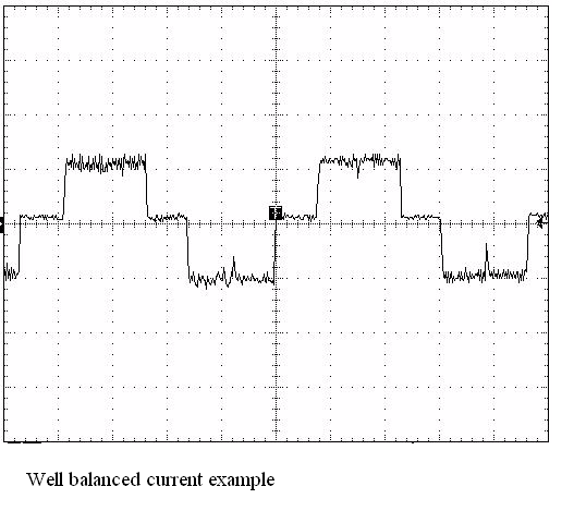
    The ideal A1 output shown below and that only occurs when PWM duty cycle is below 5%, with A1,A2,282. It seems they both get close in producing similar wave shape but is not very symmetrical even after testing various RC filtering into SAR.