This thread has been locked.

If you have a related question, please click the "Ask a related question" button in the top right corner. The newly created question will be automatically linked to this question.

INA240: Do flyback pules effect A1 precision

Guru 54077 points
Part Number: INA240
Other Parts Discussed in Thread: INA282,

Previous thread: https://e2e.ti.com/support/amplifiers/current-shunt-monitors/f/931/p/580491/2131723#2131723

Low side inductive current monitoring is prone to Delta V/t transients that should not be part of the amplified output signal yet are very present.

Datasheet header:

The negative common-mode voltage allows the device to operate below ground, accommodating the flyback period of typical solenoid applications.
Enhanced PWM rejection provides high levels of suppression for large common-mode transients (ΔV/Δt) in systems that use pulse width modulation (PWM) signals (such as motor
drives and solenoid control systems). This feature allows for accurate current measurements without large transients and associated recovery ripple on the output voltage.

That latter claim is not exactly true for 240 low side monitoring of rapidly changing periodic PWM CMMV signals.

We noticed INA282 REF1+2 tied to ground seem to block much of the flyback pulses we are seeing on the A1/A2 outputs. These cyclic pulse cycles in sync with PWM frequency (12.5kHz). That seems to hold output settling time above spec and actual sensing inductive CMMV crossing the shunt, thereby effecting SAR 75amp full scaling factor 10mv/A. Reverse or negative current below ground appears to cross PWM rejection circuit and distort the input gain scale set by REF bias pins.  The odd part is the datasheet states REF1+2 tied to GND produces Unidirectional current detection. Yet the scope captures show some inverted pulses in the ratio metric current ramp being created. It would seem that is not entirely true as it relates to isometric monotonic linear gain of CMMV.

1. How is latter possible if inverted (negative) pulses are being created in the positive current measure of so called Unidirectional current flow?

2. How can we mitigate high Delta V/t CMMV input from amplifying signals below ground and or extending output settling time from that condition?

3. Does REF1+2=GND make INA devices ignore voltages below CMMV and shunt idle mode threshold? 

4. Why does the 282 seem to better isolate the differential amplifier from low side monitoring of Delta V/t, AKA inductive flyback?

5. Are there other INA family devices with TSSOP package layout similar to A1 pin out?  

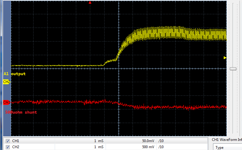
  • Perhaps datasheet 1/2 precision REF is not being correctly presented respectively REF1+2.  Notice how single triggered capture A1 output (CH2) goes positive as the shunt CMMV bounces downward to initial inductive inrush current. That is incorrect A1 output behavior relative to REF being 1/2 +1.225v and the shunt CMMV (CH1). The +/-IN input polarity of shunt has some how internally reversed! 

    The reverse output action (CH2) seems to be an anomaly not detected during lab analysis A1/A2 deviating from REF control in the differential amplifier set bias. Ideally we want positive ratio metric linear rise that follows the CMMV of inductive phase current going in the same direction.

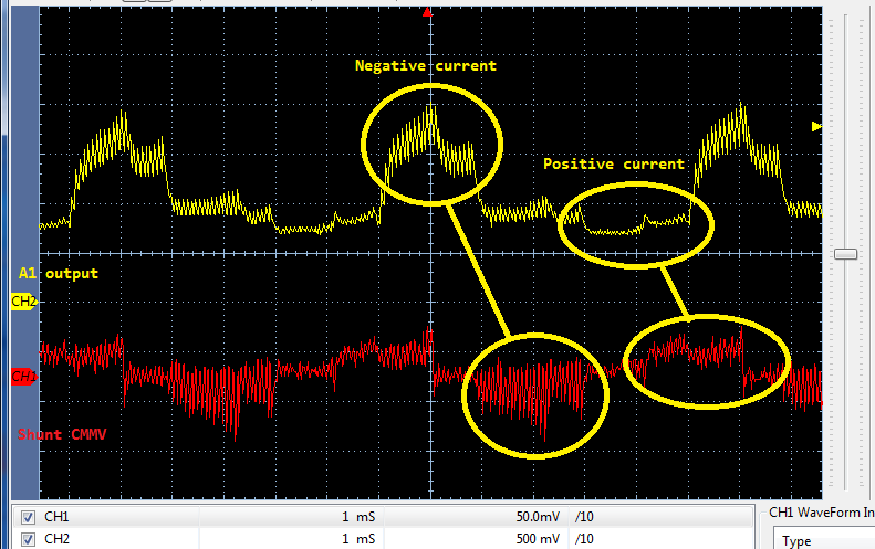
  • Perhaps even bigger issue +/-IN reversal occurring A1 output as the idle CMMV bias floating prior to each new PWM commutation. That floating CMMV gives us a clear picture in above scope capture. The output relative 1/2 REF (620mv) should not jump upward to peak 2v as clearly it has. Though we might expect some A1 output change from floating CMMV +/-IN bias lowering, it should not be as extended to VS rail.

    That would further suggest the direction of shunt current being Reverse, not Forward. How could the direction of +/-IN current flow be inverted inside the PWM rejection filter, the bigger question?

    Mechanically reversing shunt +/-IN signals seems to produce little to no transient response of the A1 output. That reversal has (+IN) connected to GND and (-IN) facing B+ in opposition to any perceived forward (positive) current flow from B+ to GND. Same behavior numerous captures indicates the PWM rejection bias circuit becomes out of phase with the valance level present on +/-IN. That behavior repeats each time the monitored CMMV bias floats slightly upward after each PWM cycle dead time in the unmonitored window.

    Thus appears A1 output being reversed and REF output bias perhaps reversed as it seems. Effectively rendering REF output bias a mute threshold respective +/-IN changes. Inverting scope CH1 overlaying CH2 lines up the shunt signal with the output signal (not shown). Very difficult for human brain to verify signal inversion but with SAR filtering on A1 output becomes bit more clear internal inversion is occurring.

  • To try to answer your questions, here is what we are thinking. First, I’d like to clarify the premise of these questions – is it that if you flip the IN+ and IN- connections, you see the same noisy behavior? I’ll assume that’s the premise and answer accordingly.
    1. This has a parallel input path through the front end. Unidirectional current flow means to us that with REF1+2=GND, and that the shunt currents that generate voltages where IN- > IN+ will not show up on the output as input * GAIN + REF, because it would be below GND. The same is true in reverse for REF1+2=V+.
    2. Schottky diodes are decent at clipping large transients quickly, and there are some MOSFET solutions too. They can’t stop transients at exactly ground but are available in reasonably low voltage options provided the current driving the transient isn’t too significant. It may not be a perfect solution but I figured it’s worth a mention.
    3. It’s not a logical decision tree determining what goes through the inputs or anything; the nature of the latter stages of the amplifier are such that they don’t drive the output below GND.
    4. The INA282 has a different architecture. It seems that in your setup with your input signals and layout that it may perform better for your application.
    5. TI does not currently have any other current shunt monitors pin compatible with the INA240 in a TSSOP-8 package.
  • Patrick Simmons said:
    . This has a parallel input path through the front end. Unidirectional current flow means to us that with REF1+2=GND, and that the shunt currents that generate voltages where IN- > IN+ will not show up on the output as input * GAIN + REF, because it would be below GND. The same is true in reverse for REF1+2=V+.

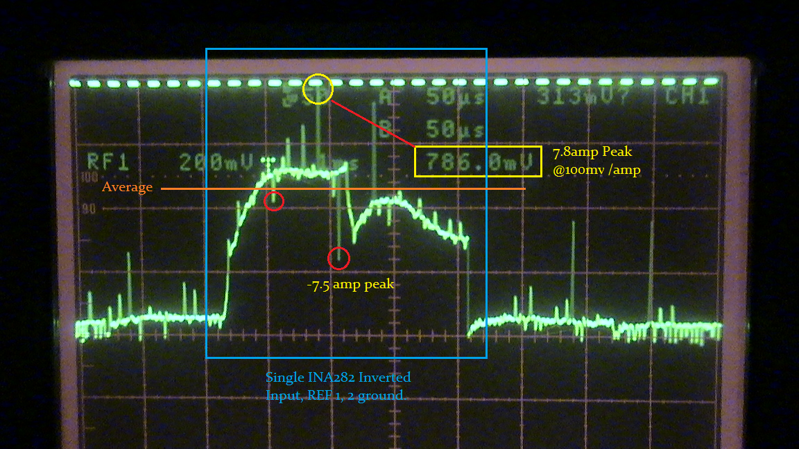
    Yet the INA282 did produce negative going pulses. It would seem that in reality INA devices do such in an undisclosed method (input * gain - inverse ^REF) We observed input CMV below ground seems to occur in output signal being an inverse delta of positive current threshold as it seemingly should! That is current reversals occur in bipolar inverters that software needs to see in order to properly control PWM duty cycles. Picture has some ground noise the SAR input filtering and SW low pass filtering clears up so they are ignored. 

    Patrick Simmons said:
    4. The INA282 has a different architecture. It seems that in your setup with your input signals and layout that it may perform better for your application.

    Forum guru past stated to try the INA240 for it's PWM/transient rejection capability. Even the 282 is depicted never with any kind of input filter as it utilizes switched capacitors chopper on the front end. 

    Patrick Simmons said:
    2. Schottky diodes are decent at clipping large transients quickly, and there are some MOSFET solutions too. They can’t stop transients at exactly ground but are available in reasonably low voltage options provided the current driving the transient isn’t too significant. It may not be a perfect solution but I figured it’s worth a mention

    Yet question was not answered, diverted away from datasheet stated facts PWM rejection stops reduces effect of transients and what of the ability to detect flyback in solenoids. Seemingly the diode you speak of is inclusive in the low side NFET body diode.  Point is CMV<50mv below ground transients perhaps are effecting the differential amplifier PWM rejection and incorrectly inverting the output transient response shown in figures 21,22. That would be a device errata the laboratory failed to test conditions exiting when VS=3v3. Above captures show an output reversal seems to occur when CMV<8-20mv and suddenly drops below, the output transient response is excessively positive when it should be negative when REF1+2=1.225v or 1/2 REF. That is not PCB layout, rather device behavior in question!    

  • It is all becoming clear what we expected in trying to achieve 75 amp full scale precision without having shunt isolation via HALL sensors exposed a can of worms. Not to say the worms can't be shocked back into the holes they came from with a proper work around, once TI acknowledges low side phase monitoring via INA devices is not without certain conditions not being disclosed in datasheets. Yet the past has proven not much being accomplished in that area other than by my efforts to make it so.