This thread has been locked.

If you have a related question, please click the "Ask a related question" button in the top right corner. The newly created question will be automatically linked to this question.

ISO122 supply voltages 5V signal

Other Parts Discussed in Thread: ISO122, LT1054

Hello,


I am planing to use the ISO122 to transfer a 0V to 5V analogue signal (not negative and only a variable static signal) from a high voltage side to a low voltage side of a PCB.

It represents the voltage of a HV-DC-link of an inverter meassured by a high restistance voltage divider (ISO122 has exactly 200k input resistance, right?). As I want to use as less space as possible I plan to use the existing power supplys of the circuitry.

This are -5V, +19V on HV side and +3.3V, +5V and +12V on LV side.

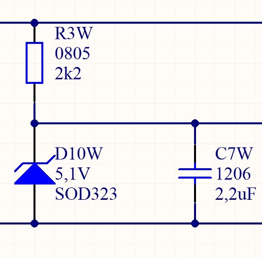
So can you recommend me the best power supply concept for my task? The 19V and -5V on HV side are generated out of a 24V supply by a 5.1V Z-Diode with a 2k2 preresistor.

I am also not 100% sure how much "extra voltage" has to be supplied, as the datasheed says not that much about rail-to-rail etc...


Thank you for your help!


Best wishes!

Thomas

  • Would it be possible to use the -5V to -Vs1, GND connected with 0V, and a zener (plus resistor) with about 12V (voltage reduction from 19V) connected to +Vs1 on HV side?


    On LV i have only positive voltages... is it possible to get propper 0V signals at Vout when -Vs2 and GND are connected to LV GND and +Vs2 is connected with +12V?


    Thank you for your help!

  • Hello Thomas,

    Yes, it is possible to connect -5 V to –Vs1, GND (pin 16 of the ISO122) to the 0 V supply point on the HV side of your board and 12 V to +Vs1.

    For the supplies on the LV side, you will need to use a similar architecture to that of the HV side. You cannot connect –Vs2 and GND (pin 8 of the ISO122) together; the ISO122 will not operate correctly with that connection. In order to observe the proper output you will need to either split your supplies in the LV side or connect GND (pin 8 of the ISO122) to a voltage that is at least 5 V above the voltage connected to –Vs2. For a 0 V input, the output will be at the same potential as GND (pin 8 of the ISO122), except for the offset voltage and noise of the ISO122.

    Note that if the difference between GND (pin 8 of the ISO122) and  –Vs2 is less than 5 V you run the risk of obtaining a clipped signal for inputs near 0V for some ISO122 units. In other words, the output (for a 0 V input) will be higher than the voltage at the GND (pin 8 of the ISO122) by a value higher than the offset voltage of the device.  

    Hope this helps.

    Best regards,

    Jose

  • Hello Jose,


    thank you for your kind answer!

    For LV side I am planing to use the LT1054. This one should create the -5V out of +5V.

    On HV side I will create the +12V out of +19V with a second zener unit (12V zener and resistor ->1k to 2k2) like the one shown above. Is this suitable for the power consumption of the ISO122?

    Thank you for your help!

    Best wishes

    Thomas

  • Hello Thomas,


    The quiescent current of the VS1 side of the ISO122 is 7 mA max. Depending on the type of zener diode used you might need to decrease the series resistor used since 7 mA causes a 7 V drop on a 1 kohm resitor; in that case there would be little current flowing through the zener.

    Perhaps it would be a better idea to ensure the zener diode is properly biased but that depends on the specific zener diode used and not on the ISO122.

    Hope this helps.

    Best regards,

    Jose

  • Ok sure, I will figure that out.

    But normally this concept should work correctly, right?

    Thank you very much for your help!

    Best wishes

    Thomas

  • Hello Thomas,

    Yes, the architecture to generate split supplies is correct.

    You are very welcome.

    Best regards,

    Jose