This thread has been locked.

If you have a related question, please click the "Ask a related question" button in the top right corner. The newly created question will be automatically linked to this question.

interferences with ISO122 output signal

Other Parts Discussed in Thread: ISO122

Hello,


I am currently using an ISO122 in my three phase inverter.

The device is used to measure the DC link voltage and transmit a proportional analogue signal to galvanically isolated low voltage side of the inverter.

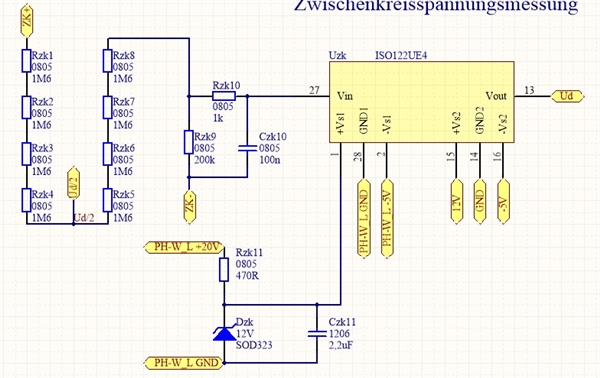
This is the schematic. A lowpass filter is located right after the voltage devider.

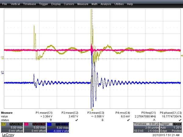
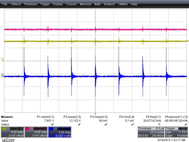
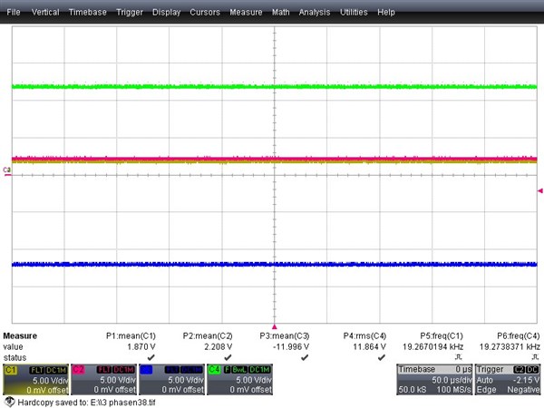
The blue voltage is the stabilized -3,3V (by Zener) supply voltage of the ISO122 (not in schematic included).

Yellow is the output of the voltage devider and red is the signal after the lowpass filter.

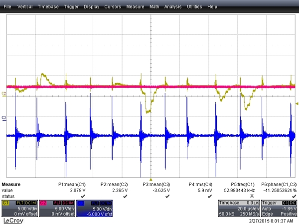
On the second picture blue is still the -3.3V supply and yellow is the output of the ISO122. (red can be ignored, as it is the heavily filtered yellow signal).

So my problem is why converts the ISO122 the red signal from picture 1 into this disturbed yellow signal of picture 2? I guess i have got some EMV issues but I am not sure where and which one. The Mosfets of the inverter are operated by 20kHz, so EMV is definitively a problem. If the PMW for pulsing the Mosfets is off, everything is fine.

Do you have any idea how I can improve the reliability of the ISO122 on my board? Do i have to add more capacitance at power supply? Or is the ISO122 simple not useable for my environment (20 kHz traction inverter)?

Thank you for any help!

Best wishes!

Thomas

  • Addition: the DC link voltage is 600V.
  • Hello Thomas,

    It seems that your PCB layout is very susceptible to the electromagnetic interference produced by the power MOSFET switching.

    I think the first issue to resolve is the excessive noise present in the negative supply of the ISO122. My recommendation would be to begin by incorporating more decoupling capacitance as close as possible to the GND1 and -VS1 pins of the ISO122. Moreover, it would be advantageous to also include several decoupling capacitors between + Vs1 and - Vs1.

    Hope this helps.

    Best regards,

    Jose
  • Hello Jose,

    thank you for your answer!

    I installed a 2u2 between -Vs1 and GND1 and a second 2u2 between +Vs1 and -Vs1. The problem is still the same. Do you think the capacitance is sufficient (2u2 1206 X7R)? Do you think i should also add more capacitance to the Vs2 pins?

    Thank you!

    Best wishes

    Thomas

  • Hello Thomas,

    Do you know what was the effect of the added capacitance? Did it decrease the ripple in the -3.3 V supply to - Vs1? If so, by how much? could you post new oscilloscope captures for -+Vs1 and - Vs1 to see how stable those supplies are?

    Your first post shows almost 24 Vpp of ripple in the - Vs1 supply and such ripple is far too large for the ISO122 or any other precision component to operate properly. If the added capacitance diminished the ripple - Vs1 the it is likely that more capacitance will help. How much additional capacitance is needed depends on what the remaining ripple is.

    Best regards,

    Jose
  • Hello Jose,

    thank you for your reply!

    Here are the new supply plots with the added capacitance:

    Yellow is still the primary (but filtered) signal, red +Vs1 and blue -Vs1.

    As you can see, the capacitance has nearly no effect.

    I tryed a little further and connected the -Vs1 pin directly with GND1:

    The noise is still the same, though -Vs1 and GND1 are directly connected...

    I guess the problem is the fact, that my voltage supply for the ISO122 and for the MOSFET-Driver are the same...

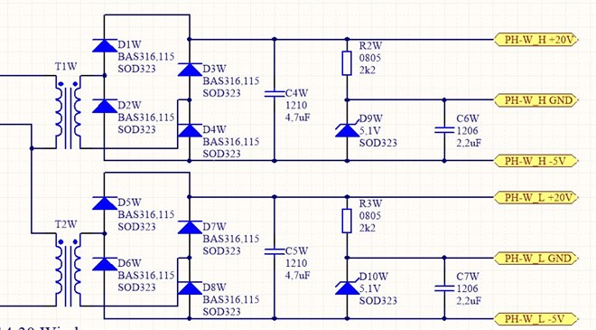
    Here is a schematic how 19V (afterwards via Z diode to 12V) and -5V (afterwards via Z diode to -3.3V) are created:

    Hope you have now enough schematics (together with the ones above) and plots to get a good overview. If you need more data please do not hesitate to tell me. Thanks in advance!


    Best wishes!

    Thomas

  • Hello Jose,

    I have changed my circuit. +Vs1 and -Vs1 are now supplied through external power supplys.

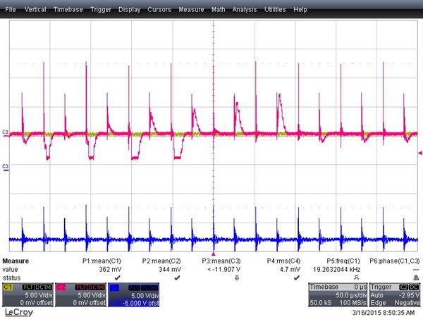
    This is the result:

    As you can see the problem is still the same (but its slightly better). The -Vs1 voltage is still very noisy, so i decided to add much more capacitance.

    (+Vs1 and -Vs1 now with 24uF instead of 2uF each).

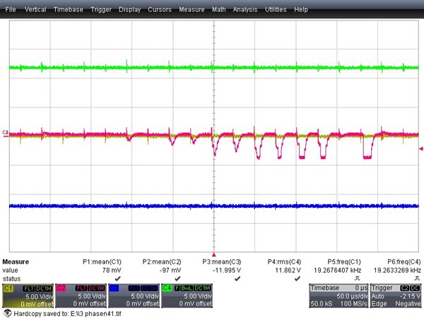
    Now I also plotted the +Vs1 voltage (green). As you can see the voltage is now much more stable but I still get these voltage drops in the output signal...

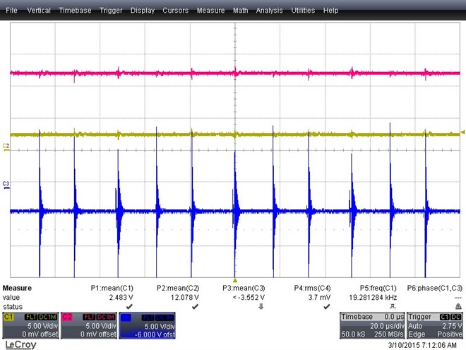
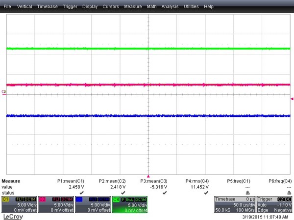
    Furthermore both voltage signals (input and output) drop to 0V. If I turn the MOSFET switching off the signals look like this:

    I guess the ISO122 is disturbed and so it pulls the input signal down to 0V (also the output signal plus adding the negative voltage drops).

    Can you please help me with this problem, as I do not know more workarounds... If i cannot solve this problem I will have to use a nonlinear optocoupler instead.

    Thanks in advance!

    Best wishes

    Thomas

  • Hello Thomas,

    Thank you very much for your latest test results. Unfortunately I do not fully understand your measurements. I will try my best to explain what I have understood in the attached document. Please read it through and correct me if I have misunderstood any point.

    150316_resp.pdf

    Best regards,

    Jose

  • Hello Jose,

    thank you very much for your effort!
    Sorry if I explained some points not that detailed.

    ZK- and PH-W_L_GND are the same potential (negative DC link). The different naming is only for schematic reasons...

    The yellow graph shows the voltage at Vin (Rzk10, Czk10 and pin 27 node) and the red graph represents the voltage at Vout. (The meassurement is of course galvanic isolated, so that GND1 and GND2 have no connection). [The value of Czk10 is actually 10nF].

    I will scope the Vs2 side as soon as possible and give you feedback.

    I am using two laboratory power supplies for +Vs1 and -Vs1. So there should be no connection between primary and secondary side of ISO122.

    I will try to add more capacitance at the points you mentioned. In previous experiments the added capacitance between +Vs1 and -Vs1 showed nearly no effect. The current capacitance between +Vs2 and GND2 and -Vs2 and GND2 are each 2u2. Let me see if an increase and a added capacitance between -Vs2 and +Vs2 will help.

    If you have more questions please do not hesitate to contact me!

    Thanks in advance
    Thomas
  • At the last point of the pdf you mention "add decoupling capacitors between +Vs2 and Gnd1, -Vs2 and Gnd1, and between +Vs2 and -Vs2."
    Do you mean GND2 instead of GND1 or is this really your intention?
  • Hello Thomas,

    Understood; thanks for the clarification.

    I did make a mistake in the sentence: "add decoupling capacitors between +Vs2 and Gnd1, -Vs2 and Gnd1, ".
    The correct statement is: "add decoupling capacitors between +Vs2 and Gnd2, -Vs2 and Gnd2, ". My apologies for the confusion.

    Since the red graph corresponds to Vout (and +Vs1 is looking cleaner, as well as -Vs1), let's concentrate on the state of +Vs2 and - Vs2. Could you please just include the oscilloscope image of the signals on the Vout side? In other words: +Vs2 with respect to Gnd2, -Vs2 with respect to Gnd2, and Vout with respect to Gnd2 (making no connection whatsoever to the +Vs1/-Vs1/Gnd1/Vin side).

    Best regards,

    Jose
  • Hello Jose,

    I added the suggested capacitances an tried a new run.

    As you can see the disturbance is nearly gone except the voltage drops at Vout signal.

    I disconnected the wires to the motor and got this scope:

    Also the Vout disturbance is gone. As I reconnected the wires the error occoured again. Actually only the connected wires cause the error, so the motor doesn't need to be connected to receive the disturbance. So i guess the EMC problem is very big and the ISO122 is very failure-prone against that. Even though it is electrically very good provided with capacitance.

    Do you have any suggestions what to do?

  • I forgott to mention:
    yellow - Vin
    red - Vout
    green - +Vs2
    blue - -Vs2
  • Hello Thomas,

    Thank you very much for posting the new results. One point that I think I have not been able to convey clearly enough is that the measurements of the +Vs2 with respect to Gnd2, -Vs2 with respect to Gnd2, and Vout with respect to Gnd2 must be taken without making any connection whatsoever to the +Vs1/-Vs1/Gnd1/Vin side. In your image above you are showing Vin next to Vout. The problem with that measurement is the possibility of having introduced a ground loop with your oscilloscope.

    You will obtain incorrect results due to ground loops in either case:
    a) connecting the GND clip of of CH2 to Gnd2 and the GND clip of CH1 to GND1, or
    b) connecting all GND clips to Gnd2 and the tip of CH1 to GND1.

    The correct method is to only measure the In side signals in one case, and only measure the out signals in the other case so that the two ground planes of your board can move to the voltages they need to move and allow the capacitive barrier in the isolation amplifier to break the undesired ground loop.

    Since you indicated that the corrupted Vout signal is present even when the motor is not connected (but I assume your power devices are switching), it seems to me that the cables in your product/board are picking up noise and such noise is directly coupled into the output of the ISO122.

    My guess (and this is only a guess; I would need to see your product in order to have a better idea of what is going on) is that the cables you mention are picking up common mode noise at a give frequency range and such noise is being injected into the output of the ISO122. In order to troubleshoot the situation I would start by measuring the common-mode current present in the cables that you mentioned and displaying such common-mode current in a spectrum analyzer. With this you can identify the problematic frequencies the cables are picking up. based on that you can target the problem by:
    a) reducing the coupling between the EMI source (probably your switching power devices) and the cables
    b) shielding the cables in order to reduce EMI pick-up
    c) Changing the length of the cables so thar they are less efficient antennas for the switching frequencies you generate from the power devices
    d) filtering the noise picked up by the ISO122 output lines or by the cables (ferrites and capacitors are the typical options here.)

    The actual combination of solutions depend on the specific constraints you have in your system.

    Hope this helps.

    Best regards,

    Jose
  • Hello Jose,


    thank you very much for your answer!

    I understand your advice to not connect GND1 and GND2 (via wire or via oscilloscope). To measure the signals I use insulated high voltage probes. So no ground loops can be created.

    My guess is also the common mode noise. The fact that the motor wires without the actual motor connected cause the noise indicates that guess...

    I will try to shorten the wires or use shielded wires. I am using new SiC Mosfets with extreme fast rise/fall times, so the wires have probably indeed the effect of an antenna.

    First I want to reduce the picked up noise of the inverter itself (wires, board, ...). Then i will reduce the disturbance of the ISO122. Can you please give me some more advice how I can filter the noise at the output of ISO122? Honestly currently I don't have that much experience in fighting down EMI problems.

    Thank you very much!

    Best wishes!

    Thomas