This thread has been locked.

If you have a related question, please click the "Ask a related question" button in the top right corner. The newly created question will be automatically linked to this question.

XTR117 wiring queries

Other Parts Discussed in Thread: XTR117, LM35, OPA317, TINA-TI, OPA344, OPA340, LMC6081, OPA347

I am trying to wire LM35 output to XTR117. What I am trying to do is to generate 4-20mA current. 4mA for minimum 25 Degree C and 20mA for 80 Degree C of temperature. The respective output of LM35 would be 250mV and 800mV on which I have applied gain of 5 by using a single supply opamp. So the voltages would be 1250mV and 4000mV which is sufficient for full scale recommendation. Now , how to make sure minimum 40uA at 25 Degree C at amplified input of 1250mV and 200uA at 80 Degree C amplified to 4000mV after input offset given in Figure 2 of datasheet of XTR117. If I need to skip input offset using Vreg output then how to scale the inputs accordingly ?

  • Hello User,

    The circuit below provides positive gain and a negative offset to translate the 250mV - 800mV output of the LM35 to a 1V - 5V output which is easily accepted by the XTR117.  Use the exact component values shown below.  The OPA317 is a dc accurate op amp that has good swing to the positive rail and should be used for this application.  If other amplifiers are used, please be aware that their current consumption must be less than 3 mA for proper operation of the transmitter. The simulation file can be opened in TINA-TI SPICE which is a free SPICE simulator offered by Texas Instruments.  Decoupling capacitors should be added to all device power supplies as recommended in their datasheets.

    XTR117+LM35.TSC

  • If I would like to change the span of measurement say 10 degreeC to 100 degree C or for an o/p of 100mV to 1000mV....then where shall I make variations for that ? In my opinion Rset and feedback resistors of OPA317. Correct me if I am wrong.
  • The gain and offset of the circuit would both need to be adjusted to accommodate for the change in input offset and span.  This requires scaling all of the circuit components which was a little complicated.  I attached a .pdf of the math I performed to calculate the gain (m) and offset (b) of the circuit transfer function and then the equations to calculate the circuit component ratios.  If the parallel combination of R1 and R2 is much smaller than RG then the equations get a lot simpler.  Once the ratios of RF/RG and R1/R2 are known you just need to find the best matches you can with standard component values that maintain the relationship that R1||R2 << RG.

    Here's an updated image of the circuit and simulation file with the components labelled the same they are in the calculations.

    8304.XTR117+LM35.TSC

    Calculations:

    Mathcad - Calcs.pdf

  • Hi there, I ran simulations and found it very useful, Can you please suggest me PDIP replacement/Equivalent for OPA317 opamp ?

  • Hello,

    There is not a direct replacement for the OPA317 in a PDIP package.  Some other devices that would work in this application and are available in the PDIP package include the OPA340, OPA344, and LMC6081.

  • I bought OPA347 from local distributor....almost similar specs....let me try....hope it works....I will get back if I get something new.

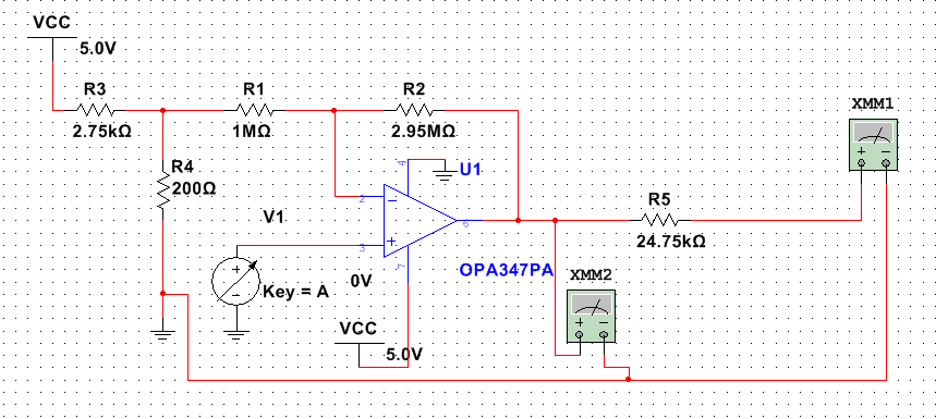
  • I simulated this on Multisim as well as TINA and it worked fine. Now I am changing the input from sensor or Vopa ranged for 0 to 1000mV (0 degree to 100 degree centigrade). Attaching the schematic here for your reference. Can you tell me whats wrong in it? As per calculation I am getting voltages, but as per simulation I am not getting desired result. Even if I am changing range to 100mV to 1000mV then also simulation shows wrong output.  

  • I just referred to SLOA097 article and I have rectified my mistake related to scaling. Thanks for helping throughout. Now its working good in simulation.