This thread has been locked.

If you have a related question, please click the "Ask a related question" button in the top right corner. The newly created question will be automatically linked to this question.

TINA/Spice/TL084: TL084 as 16-bit ADC driver for TMS320F28377D

Part Number: TL084
Other Parts Discussed in Thread: TINA-TI, , THS4531

Tool/software: TINA-TI or Spice Models

Hi All,

I am using TMS320F28377D for my inverter application. I need to use 16-bit ADC to get precise result. So, I have to use differential configuration there is no other option. My sensor output is buffered single ended signal. First of all i need to convert it into differential foam. For that particular application,I am using TL084 OPAMP to do this task. One sensor output(VoutP) is directly applied to ADCINA0 and another(VoutN) is subtracted from 3.3V (Which is VREFHI for my controller) and then applied to ADCINA1 . So I can also maintain my common mode requirement which is 1.65V (Vcm = (VREFHI + VREFLO)/2).  At every instance my common mode voltage is maintained.For E.g., VoutP=2.2V then VoutN=1.1V and Vcm = (2.2+1.1)/2 = 1.65V.

Figure 1 is simulation circuit and figure 2 is output.

Now, my question is "Is it right method to do this task?". Can i apply this differential signal to ADC?

See following thread : e2e.ti.com/.../2100577

Figure 1:

Figure 2:

Thanks and Regards,

Maulik Timbadiya

  • Hi Amtech,

    The circuit you've shown relies on the input (VoutP) CM of 1.65V to be held constant and match the bias you've provided to the TLO84 non-inverting input. If you are using a 16 bit ADC, I'm not sure you can guarantee this matching and tracking. For this level of accuracy, you'd probably have to consider some offset and gain trimming scheme for your circuit.

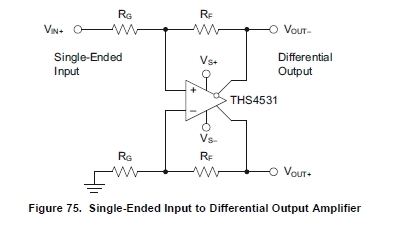
    For driving the differential input ADC, a better solution would be to go to a Fully Differential Amplifier (FDA) as was suggested to you in the link you provided:

    Let me know if you need help with that?

    Regards,

    Hooman

  • Hello,

    In addition to Hooman's comments take a look at TIPD131 which describes the design of a similar circuit to the one you were suggesting.

  • Dear Hooman,

    You mean to say that i should go with THS4531? Right?

    Can i get accuracy if my sensor output is previously buffered by TLO84 and then i convert it into differential by ths4531??

    Which OPAMP parameters that i need to take in account when dealing with result accuracy?

    Thanks and Regards,

    Maulik

  • Hi Amtech and Collin,

    To reply to your questions:

    Question: Which OPAMP parameters that i need to take in account when dealing with result accuracy?

    Response: It kind of depends on your application. The ADC will interpret any differential input as a signal which, if unintended, will become an error. Additionally, there are specs on how much CM deviation can be tolerated between the differential analog input.

    Question: Can i get accuracy if my sensor output is previously buffered by TLO84 and then i convert it into differential by ths4531??

    Response: Using the THS4531 would alleviate your circuit's issue with CM tracking / mismatch between VoutP and VoutN as the CM loop internal to the THS4531 would ensure tracking. If your sensor signal can drive the Single Ended to Diff stage you build using the THS4531 directly, you would not need the TL084 buffer either. It all depends on the input impedance you design for and what the sensor output impedance / current-handling capabilities are. Let me know more details about your sensor if you like me to help you design this circuit.

    Question: Which OPAMP parameters that i need to take in account when dealing with result accuracy?

    Response: For a 16 bit data acquisition system, you would want your error terms to amount to no more than 1/2 LSB. So, you have a very tight spec to work with. The static errors (offset, bias current, etc.) may be errors that you can take-out using one-time, or occasional calibration. The dynamic / shifting errors (offset drift, bias current error variation over temp., etc.) may be more difficult to factor-out.


    Resistor matching between the two halves of your circuit (RF, RG) is very important. If I know more details about what your needs are, we could put the design into TINA-TI and run some scenarios to see if the error terms need to be improved.

    Please let me know.

    Regards,

    Hooman

  • Hi Amtech,

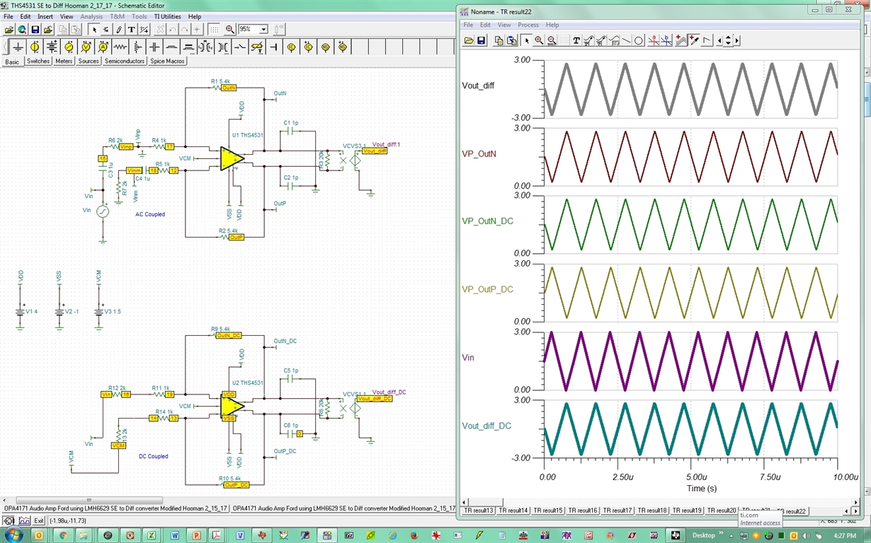
    Here is couple of implementations using a FDA (THS4531), to see if this is what you're trying to achieve?

    I've assumed an arbitrary sensor impedance (2k) because I don't know what you have? I also don't know if your sensor can deliver the peak currents required? If not, the input impedance would have to be increased or the sensor should be buffered.

    Also, I've AC coupled the input signal (upper implementation) to simplify any CM errors / matching if you don't need the sensor DC information? The lower implementation, is DC coupled and assumes that the sensor output CM voltage is closely tied to the VCM of your ADC [ = (Vreflo + Vrefhi)/2 ] of 1.5V in this design.

    To swing from 0V to 3V, I've used the THS4531 with a slightly negative Vss (= -1V). Otherwise, you cannot swing exactly to 0V.

    Here is the TINA-TI file for reference:

    THS4531 SE to Diff Hooman 2_17_17.TSC

    Regards,

    Hooman

  • Thank you Hooman,

    Your TINA model is working fine.

    But i have a question "datasheet is saying Vs- to Vs+ maximum rating is 5.5V, then why TINA model is accepting any value without any warning?"

    For e.g., +5V to Vs+ and -5V to Vs- wouldn't generate any warning.

    Regards,

    Maulik

  • H Amtech,

    You are correct in that Transient (or AC response) analysis with TINA-TI (or Pspice equivalent) will not show any warnings if you exceed the device operating supply voltage range. I think that's true for every amplifier I have seen before. It's up to the user to ensure that they do not violate the device specs.

    Most macro models do however correctly depict the output swing (relative to the V- and V+ rails) and output current capability.

    Regards,

    Hooman