This thread has been locked.

If you have a related question, please click the "Ask a related question" button in the top right corner. The newly created question will be automatically linked to this question.

TLV9062: how to improve crossover distortion and distortion

Part Number: TLV9062
Other Parts Discussed in Thread: TINA-TI

Dear Specialists,

My customer is evaluating TLV9062.

He is encountering crossover distortion and distortion.

I would be grateful  if you could advise.

---

I am considering TLV9062 for widening bandwidth and reducing current consumption than previous model.

However,  crossover distortion is observed less than 1kHz.

Around 3kHz, distortion is observed.

More than 5kHz, it still distorted.

I'd like to know how to improve crossover distortion and distortion.

---

I appreciate your great help in advance.

Best regards,

Shinichi

question about TLV9062.pptx

  • Hello Shinichi-san,

    Cross over distortion occurs when the input stage of the amplifier switches from the PMOS transistors to the NMOS transistors. When this transition occurs there is a shift in performance of the device, such as a change in offset voltage, a decrease in bandwidth of the device, or noise. The shift in performance is what causes the increase in distortion.

    Cross over distortion can be avoided if only the PMOS region of the input stage is used. For the TLV9062 the input common mode must be between (V-)-0.1V and (V+)-1.4V to avoid cross over distortion.

    You can identify the PMOS region of an amplifier and avoid cross over distortion by looking at the common-mode rejection ratio (CMRR) test conditions. Notice that the CMRR specification is higher for the test condition with the common mode voltage between (V-)-0.1V and (V+)-1.4V. The CMRR spec is higher in this region because the input stage does not cross over into the NMOS region.

    You can also determine where the NMOS stage becomes active by looking at the figure Offset Voltage vs. Common-mode Voltage (Figure 4 in the TLV9062 datasheet). Notice that at a common mode voltage above (V+)-1.4V there is a shift in offset voltage, this is where the NMOS region becomes active.

    Since the common mode voltage of the amplifier is fixed at ~280mV I do not believe the customer is seeing cross over distortion.
     
    For more information on cross over distortion I recommend watching our TI Precision Lab videos on Low Distortion Design.

    What may be occurring is the customer is seeing some non-linearity due to the output swing of the amplifier. The output is specified 60mV from the rail with a 2k load. Please see the Aol test conditions. In the customers circuit the lower portion of the output signal is attempting to go below 60mV. As frequency increases the gain also increases because the AC coupling caps are getting closer to a short. This causes the output to attempt to go even further below the 60mV limit at higher frequencies.

    To test out my theory, can the customer increase the biasing voltage to the non-inverting input to 1.1V (mid-supply)? They can increase the biasing voltage by increasing resistor R1 in the schematic you provided to 560k ohms.

    Lastly, in the 10kHz measurement in the presentation, why are the amplitudes of the other suppliers device and the TLV9062 different?

    Thank you,

    Tim Claycomb

  • HI Timothy,

    Thank you for your reply.

    I'll share your suggestion with the customer and make him try.

    The reason there is the difference between another supplier and TLV9062 at 10kHz, The bandwidth of another amplifier is not enough( only a few kHz).

    If he has an additional question, I consult you.

    I appreciate your great help.

    Best regards,

    Shinichi

  • Shinichi,

    One or both of these suggestions should help improve signal.
    Try a capacitor to ground on the noninverting input to keep reference voltage clean.
    Lower the noninverting voltage by 200mV.

    I incorrectly thought the input common mode was 1.1V in the application.

    Because the 2nd amplifier can clip, I suspect noise injected on reference voltage via input to input pin capacitance.  

  • Hi Ron,

    Thank your for your comment.

    I'll share your suggestion with the customer.

    I appreciate your great help.

    Best regards,

    Shinichi

  • Hello Shinichi-san,

    If our responses have solved the customer's issue please click the green "This Resolved My Issue" button.

    Thank you,

    Tim Claycomb

  • Hi Timothy,

    My customer has an additional explanation and a question about your answer.

    I would grateful if you could advise.

    ---additional explanation

    I'm sorry for lack of explanation.

    The input waveform is measured at function generator output by AC coupling, not at invert pin.

    Could you please see attached file.

    Actual input level at invert pin is 280mV(center) +/-10mV.

    In this case, is there any difference about the answer.

    --- additional question about output waveform

    The output distortion is observed not only the bottom (less than 60mV) you mentioned, but also top of the waveform.

    What is the reason and work around?

    ---

    I appreciate your great help and cooperation.

    Best regards,

    Shinichi

    measured point.pdf

  • Hello Shinichi-san,

    Thank you for the diagram clarifying the measurement point.

    This does not change my initial answer, I still believe that the issue the customer is seeing is caused from the output limitations of the device. To show what I mean by the amplifier is attempting to output a signal below the output swing specification I put the customer's circuit configuration into TINA-TI using an ideal amplifier and ran a transient analysis with a 10kHz input. Please see below and attached TINA-TI file. As you can see the output signal goes down to -210mV which is well below the output swing specification of the device and even below V-.

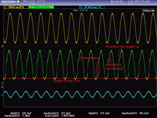
    The reason the top of the waveform appears to also be distorted is because when the output attempts to go below the output swing specification the the amplifier goes into overload recovery. When the amplifier goes into overload recovery there is a delay between the input changing and output changing (called overload recovery time in the datasheet). Once the device comes out of overload recovery the output signal attempts to catch up to the input signal which is why you see a linear output on the rising edge of the output. The output does not "catch up" to the input until it is near the top of the output waveform. These different regions are easiest to see in the 3kHz measurement. Below shows each region, linear, catching up, and caught up to help clarify my explanation.

    Thank you,

    Tim Claycomb

    Ideal Amplifier.TSC

  • Hi Tim,

    Thank you for your reply.

    I sent your suggestion to the customer and he could understand influences of the overload.

    And then he changed the input signals in order not to be overload, but they were seen overload and cross over.

    I would be grateful if you could advise what is the problem.

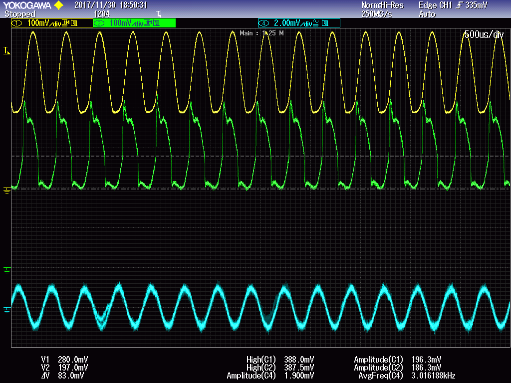
    (1)    Vin:2mV, f:3kHz

    This waveform may be affected by overload.

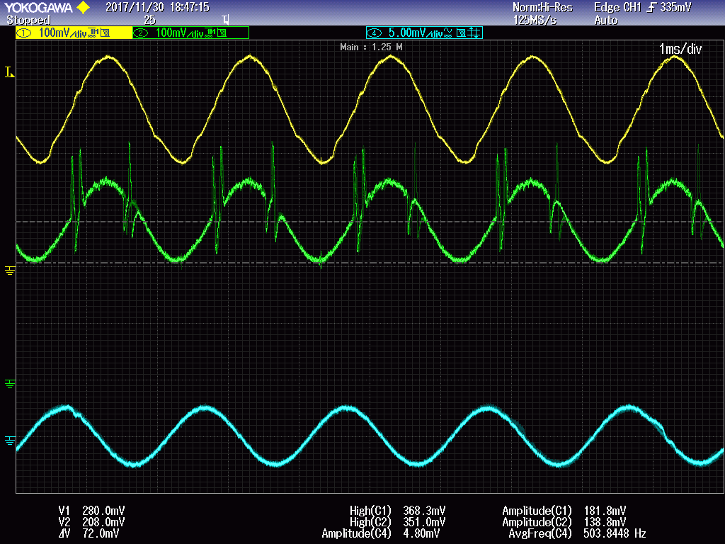
    (2)Vin:5mV, f:500Hz


    Disturbance is observed in the measured waveform near zero cross over.

    ---

    I appreciate your great help.

    Best regards,

    Shinichi

  • Hello Shinichi-san,

    I apologize for the delay in a response. I have just returned from international business travel and I will look into the customers issue as soon as possible.

    Thank you,

    Tim Claycomb

  • Hello Shinichi-san,

    Can the customer please provide a screen shot of the non-inverting input with the input and output signals? It would be helpful if the scaling of the vertical axis is set as small as possible. Please AC couple the measurement if needed. I would like to see if there is some noise on the non-inverting input.

    What is the part number of the competition device? If you cannot provide the part number please tell me the bandwidth of the competition device. If the bandwidth of the competition device is significantly lower than the TLV9062 the distortion the customer is seeing may be filtered out due to bandwidth limitations.

    Does the customer have decoupling capacitors placed directly next to the supply pins? We recommend using 0.1uF decoupling capacitors placed directly next to the supply pins.

    Can the customer remove R11 and test the output of the 1st amplifier? I would like to see if the second amplifier has any effect on the waveform. Removing R11 will remove the second amplifier from the signal chain and help me determine if the second amplifier has an effect on the first amplifier.

    Thank you,

    Tim Claycomb

  • Hi Tim,

    Thank you for your reply.

    About your request, I'll ask the customer confirm.

    (1) A capture zoom in at non-inverting input

    (2) competitor device number

    (3) decoupling capacior value

    (4) waveform removed R11

    I'll let you know I get them.

    I appreciate your great help and cooperation.

    Best regards,

    Shinichi