This thread has been locked.

If you have a related question, please click the "Ask a related question" button in the top right corner. The newly created question will be automatically linked to this question.

LMV612: Bias current, offset current, input pin internal protection diode

Part Number: LMV612
Other Parts Discussed in Thread: LMV931-N, LMV341

1. What is the maximum value of the bias current and offset current? There are only typical values (15nA and 13nA) in the manual, and there is no maximum.

2. Does the input pin have an overvoltage protected diode?


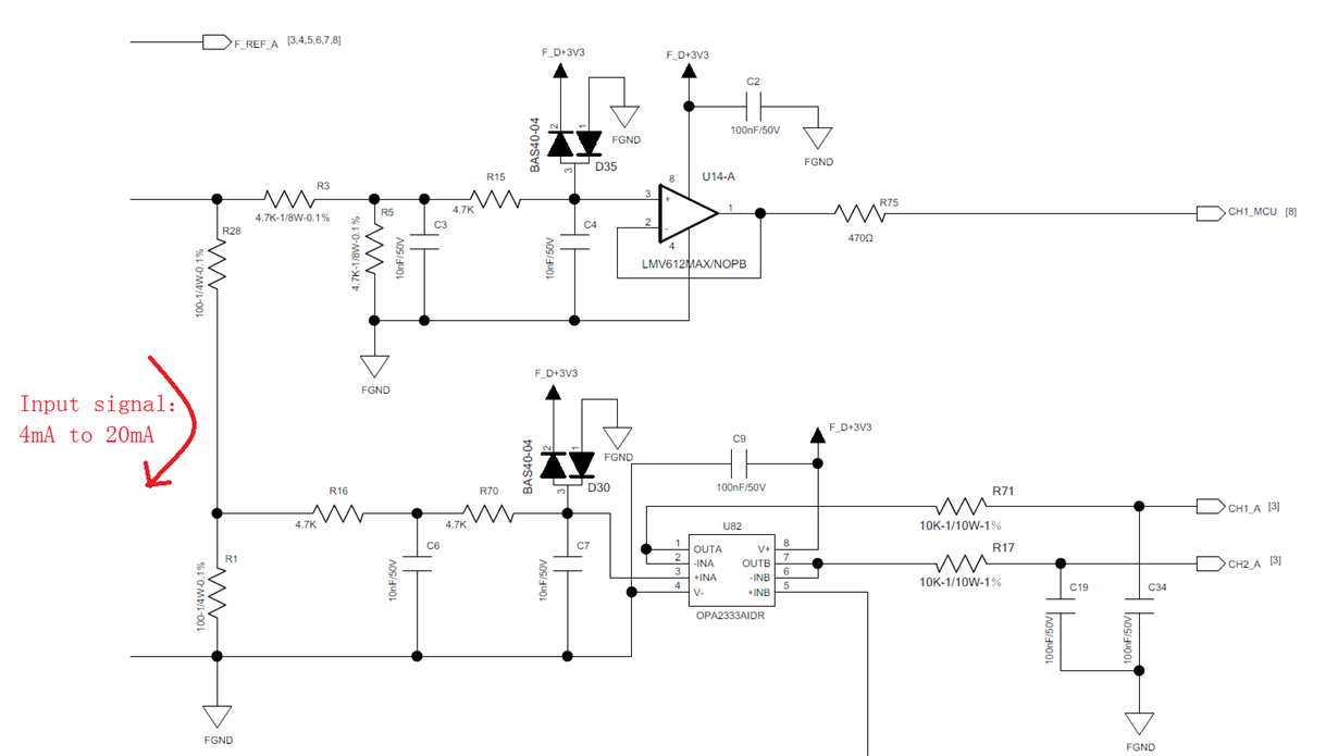
Pictures R1 and R28 are 100Ω precision resistors that convert a 4 to 20 mA signal into a voltage signal.

In order to minimize the influence of the precision resistance acquisition current signal, R3 and R5 are modified to 1MΩ, and the LMV612 bias current and offset current affect the signal accuracy.

  • Hi Rengui,

    If there is no maximum value given in the datasheet for bias current and offset current, then it is not a tested and guaranteed value. The typical value encompasses ±1 standard deviation from the mean of the parameter value, so ~68% of devices will be encompassed by the typical spec.

    In section 7.2 of the datasheet, you can see the functional block diagram and the included ESD diodes. There are diodes to VCC and VEE. It is recommended to not turn these on and to use external protection components if you are concerned about electrical overstress conditions in your design.

    -Paul
  • Hi Rengui,

    If you'd like similar devices with specified maximum values for the parameters you're looking at, look at the LMV341 and the LMV931-N. Those devices have similar electrical performance characteristics and have more testing done (which will guarantee that the device will meet the spec in the datasheet).

    Best,
    Paul