This thread has been locked.

If you have a related question, please click the "Ask a related question" button in the top right corner. The newly created question will be automatically linked to this question.

OPA2140: Thermal management or how do I estimate junction temperature?

Part Number: OPA2140

I am using OPA2140 (SOIC) in my design. In one of the positions it supplies a fairly high current (up to 9mArms) and power supplies are +/-15V i.e. 30V rail to rail. I calculated the power on the IC as ~200mW in my circuit.

Problem is I do not know how to use the thermal information on the data sheet, reproduced below, to estimate the junction temperature, even after reading the application report mentioned there.

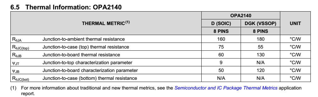
So... How may I estimate the junction temperature for a 55°C ambient temperature? I guess it also depends on the layout, so what is the recommended layout, how much copper etc. to achieve a safe junction temperature. By the way, what would be a safe worst case Tj?

Thanks in advance.

  • Hi Elder,

    Are you familiar with the Precision Labs video series? This video is on this topic. training.ti.com/ti-precision-labs-op-amps-power-and-temperature

    Best regards,

    Sean
  • Hi, Sean.

    Thank you for your fast response and the heads up on the precision labs video.

    I am already familiar with the concepts presented in that video though. The problem is I do not know the criteria used to determine the Theta parameters (especially J-A) in the data sheet. Delta-T with that value and 200mW power is 32°C which is OK and, at a 55°C ambient temperature, gives a good margin from the IC maximum (though I would prefer to lower that temperature by 10°C). However, what is the PCB characteristics to (copper area, weight and layout) obtain that thermal performance?

    Psi-J-B hints the junction-to-board Delta-T is 10°C; so, what would be the PCB area and how should it be laid out to obtain the remaining 22°C? BTW, what is the difference between Psi and Theta-J-B?

    Again, thank you for your support.
  • Hi Elder,

    The equations for Theta parameters are simply thickness/(conductivity*area) with units °C/W. However, many Theta parameters add in parallel while dissipating heat. Psi JB is (Tj - Tcenterpin)/(power dissipation) measured empirically. This includes all parallel resistances, and therefore is an easier metric to project junction temperature from pin temperature, although it is not a true thermal resistance.

    To achieve a Theta BA of (22°C/200mW)=110°C/W or less, you can calculate a theta parameter for your board. Using a conservative thermal conductivity for air of 1400 (°C W^-1 cm^-2), a 14 cm^2 board would give a thermal resistance of 100°C/W considering conduction only. Convection and blackbody radiation will decrease this estimate if taken into account. You can decrease this value by adding a heat sink and a fan. The main layout consideration is effectively getting the heat into the ground plane; at steady state the thermal mass of the board should theoretically not matter. (In practice, a ground plane is not a node and therefore will have a 2D temperature gradient, where each point will conduct+radiate power proportional to its temperature.)

    Best regards,

    Sean
  • Hello, Sean,

    Thank you very much for the hints. They give me something to work with.

    Regards.

    Elder.