This thread has been locked.

If you have a related question, please click the "Ask a related question" button in the top right corner. The newly created question will be automatically linked to this question.

INA125: INA125P giving a different reference voltage than what is being given in the data sheet

Part Number: INA125
Other Parts Discussed in Thread: INA126, OPA191,

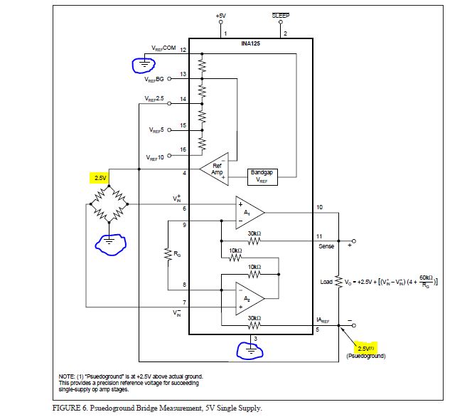
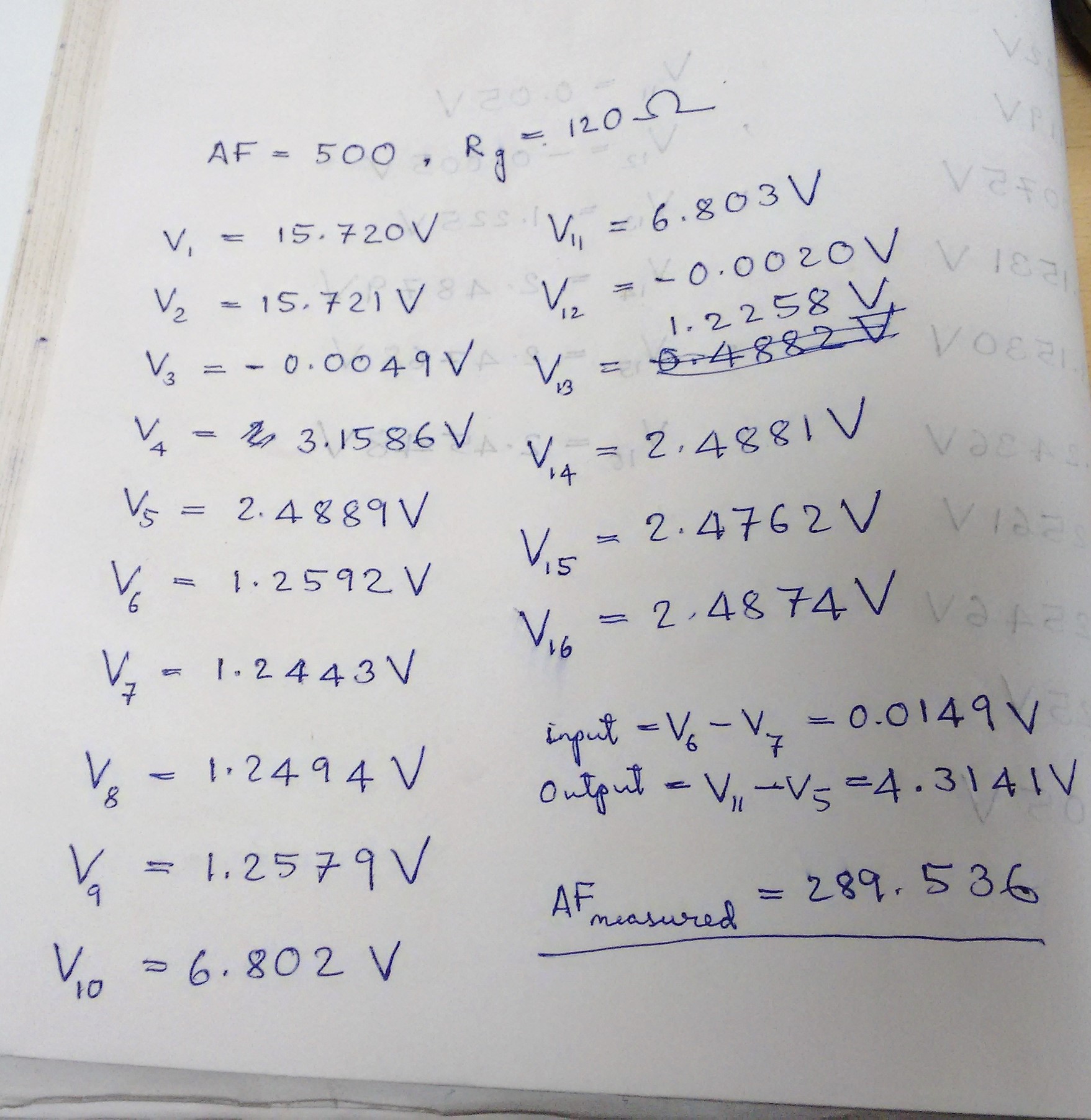
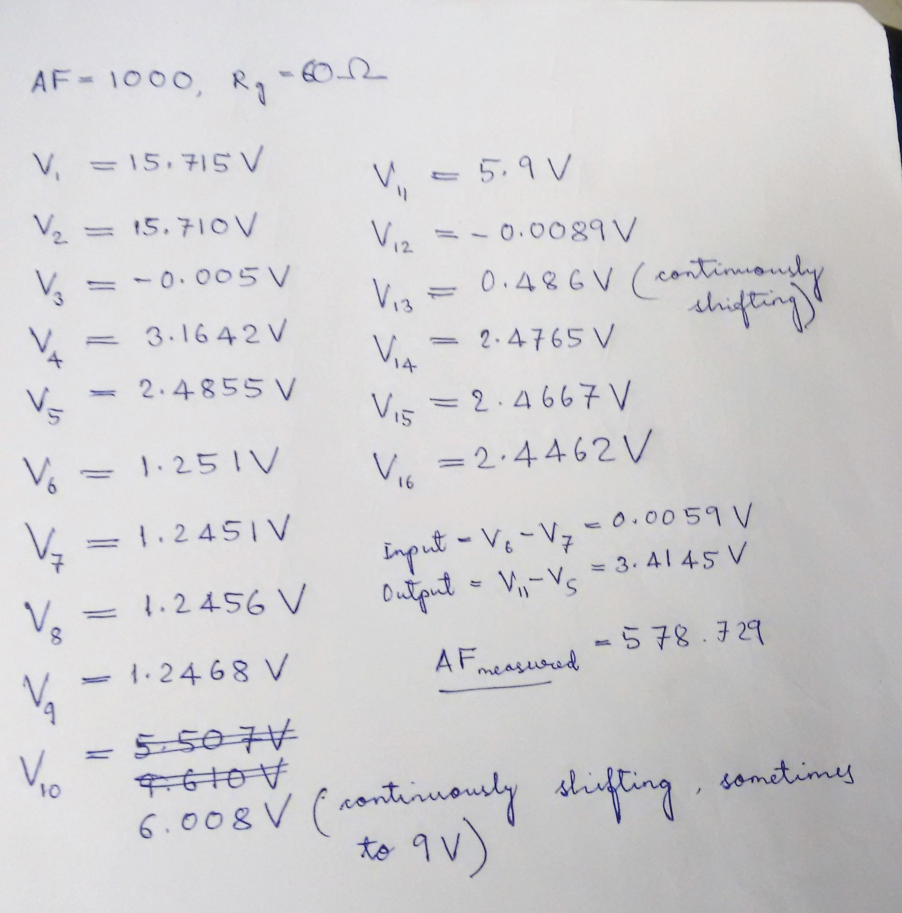
For the last six months, I have been using INA 125 P amplifier. The problem I am facing is that in figure 6, page number 13 in the datasheet, pins 14 and 4 have been connected and due to this connection, we would be getting a reference voltage of 2.5V (as is shown in the figure). Experimentally, I also made the same connection but I am getting a reference voltage of 1.44V. Why this anomaly is happening when everything is correct in my circuit? Please help.

  • Hello,

    Please post a copy of your schematic for us to diagnose the issue.
  • Hello Zak,

    I am attaching the schematic herewith

    I have exactly made these connections. But my problem is that in the highlighted regions, I am getting a voltage of 1.44V instead of 2.5 volt. Pins 12,3 have been connected to the ground of the Wheatstone bridge. And at pin 1, I am supplying a voltage of 5V as is given in the data sheet. Pin 2 has been connected to pin 1.

    My problem is that I want to get 2.5 V as the voltage which excites the Wheatstone bridge.

    Regards,

    Captain

  • Zak,
    I am uploading the schematic diagram but on posting, the diagram is not coming. I tried a couple of times. So, can you give your mail id so that I can mail you straight away the diagram. If not, can you suggest some other means?

    Saurav
  • Zak,
    This time it has come. I hope my problem is much more comprehend-able now.

    Captain
  • Hi,

    What is the resistance of your bridge? If you disconnect the bridge do you see the expected 2.5V output?
  • Zak,

    The effective resistance (or equivalent resistance) of my bridge is 109.091 ohm. And if I disconnect the bridge, I do get the expected 2.5 volt.

    I am attaching herewith the diagram

    So, what should be the net resistance of my bridge so that I can get the expected 2.5 Volts or any other reference voltage as given in the datasheet.

    Regards,

    Captain

  • Normally, the datasheet should specify what the drive capability of the reference is, but for some reason this was not done for the INA126. I can confidently say that 100 Ohms is too low of a bridge resistance for the reference to drive (would require roughly 25mA), but it is difficult to say what the minimum resistance you need would be. If you have the flexibility to increase your bridge impedance I would suggest increasing to over 2.5kOhm so that the reference doesn't need to supply more than 1mA (this is generally a safe limit for a reference).

    Alternatively, you could add a transistor as in figure 4 in the datasheet to boost the output current.
  • Hi Zak,
    Due to some experimental constraints, it is almost impossible for me to increase the impedance of the bridge to 2.5 kilo ohms. Of course, I would consider using the transistor and come back to you.
    But for my present problem, where I need to get high voltages (between 2.5 to 10 volts) to excite the Wheatstone bridge, can you suggest any other instrumentation amplifier or operational amplifiers, where I could get these voltages with the present bridge impedance of 109.091 ohms.
  • If you're trying to get 10V across ~100 Ohms then you need to source 100mA and to get that you'll have to start looking at power op-amps. However, a power op-amp is not going to have very good dc performance. I don't have anything to offer that is going to have an on-board reference capable of driving that bridge. If you don't want to boost the current with a transistor, then you could consider using a device like the OPA191 to buffer the reference. This is an op-amp with a 65mA max output current and good dc precision. My recommendation would be to run the bridge with a lower voltage (closer to 2.5V) and split the gain into multiple stages if needed.
  • Hai Zak,
    In figure 4 of the datasheet of INA 125, the transistor that you people have shown is TIP29C. But two different types of TIP29C's are available in the market. In one of the TIP29C's, the hFE is 75 and in the other, hFE is 15. Rest all the parameters are equivalent or same.

    Can you suggest, out of these two, which one would be better for solving the problem that I am facing.

    Secondly, could you elaborate more, that how putting a transistor, can increase the bridge impedance to 2.5 kilo ohms without making a significant potential drop, as is in the case of a high value resistance. i.e it would increase the impedance but there would be significant potential drop across it, thus further reducing the voltage required to excite the bridge.

    Regards,
    Captain
  • Generally speaking the hFE of the transistor is not critical and will tend to fluctuate pretty heavily. A larger hFE just means you have greater dc current gain, so you don't have to drive as much current into the base to get the desired output current. You should be fine with either transistor, but since we are unsure what the drive capability of the reference is, if you want more assurance then choose the version with higher hFE.

    Adding the transistor does not increase the impedance of the bridge, it increases the impedance seen by the op-amp and supplements the output stage of the op-amp with a transistor capable of higher current output. You don't necessarily need to use the TIP29, you just need a transistor that can tolerate the maximum current you intend to source to your bridge and that has a breakdown voltage greater than your supply. As long as you make the connection as shown in the datasheet then the transistor is in the feedback loop of your op-amp, and thus does not contribute any significant error to the reference voltage across the bridge.
  • Hi Zak,

    After yesterday's reply, I tried with a different transistor in place of TIP29C. The transistor that I used was 2N2222.  My first question is that I couldn't understand the circuit diagram of figure 4, involving the transistor. (which I have attached herewith). Emitter and base portion is clear but in the collector region, only V+ is written. I want an excitation voltage of 2.5V. So, what should the appropriate value of V+. and where to connect V-?  Is V- connected to the pin 4 as shown by blue line in the diagram?

    Please suggest

    Regards,

    Captain

  • V+ is the positive supply that you intend to pull the additional current from. This will likely just be the same supply you are using for the INA125, but you should still make sure that the supply can provide the current you need to source to the bridge. The supply must be greater than your bridge reference voltage because some voltage must drop across the collector to emitter for the transistor to function. This voltage will be the difference between your V+ and the bridge voltage, so you must make sure you remain within the power dissipation limitations of the transistor.
  • Hi Zak,

    First of all, thank you very much. You had been replying all my queries one after the other.

    I have connected the V- of the power source to the ground and the V+ to the collector as shown in figure 4 of INA 125 datasheet. So, now, I get the excitation voltage as is given in the datasheet. i.e.(2.4786  volts)

    But now, I face another problem, my Rg (between pins 8 and 9) is 1kilo ohm. So, I get an amplification factor of 65. But when I make Rg equal to 120 ohm, I do not get the amplification factor of 500. It gets saturated at 1.18 volts. My input voltage to  the amplifier is 11mV. So, after amplification, the voltage should be 5500mV but what I get is 1180 mV. My supply to the INA 125 and transistor is 5 volts. Why is this happening? Please help.

    Regards,

    Captain 

  • Hi,

    No problem, that's what we're here for!

    Is this an ac or dc input signal? With a gain of 500 your bandwidth is limited to 900Hz, so if your signal is changing any faster than this there will be attenuation. Additionally, the output swing of the INA125 is only within about 0.8V of the positive rail (1.2V min), meaning for a typical device you can't get closer than 4.2V to the rail (or 3.8V min). If you are making the connections as shown in previous posts, then your negative output terminal is raised to 2.5V to begin with, meaning you could only accomodate an increase of about 1.3V to 1.7V before you run into the output limitations. I believe this is the root of your issue.
  • Hi Zak,

    The signal that I want to amplify is a dc input signal. So, I think there won't be any question of bandwidth for my problem as frequency is zero Hertz. I didn't understand the second and third lines of your reply.

    So, once again, I am just telling you that my Rg is 121 ohm. So, AF is 500. My input voltage to the amplifier is 10-12 mV DC. So, after amplification, the voltage should be 5000-6000 mV DC. But the voltage that I get after amplification is less than the theoretical value. The supply to the transistor and the amplifier is 5 volts.

    Just I would give an instance.

    Input voltage to the amplifier=10 mV DC

    Output amplified voltage=3.1 V DC

    For this instance, I would just give the voltages of each pin with respect to ground

    So, can you suggest me how I can get the desired output amplified voltage that matches with the theoretical value.

    The connections are all same as discussed in the previous posts.

    Regards,

    Captain

  • There are a couple issues here and I will try to explain as best I can:

    1) The voltage you have measured at pin 5 suggests you have not tapped the transistor at the emitter, but rather the output of the reference voltage op-amp. The 2.5V transistor output is the accurate reference that you want to use. However, if you are only applying a dc signal that will never change polarity, you don't even need to bias the output to a pseudoground as done in figure 6, and you can have your load reference to ground. See below for a comparison:  

    2) You can't expect your output voltage to exceed, or even equal your supply voltage. No op-amp can truly swing all the way to the supply rail. Biasing pin 5 means that pin 10 must go to IAref + 5V, which means you need an even greater supply voltage. So if you have 2.5V at IAref, then the output needs to swing to 7.5V to produce a 5V differential output. On top of that, worst case the INA125 can only swing to within 1.2V of your positive rail, meaning in that same scenario you would actually need a supply voltage of 8.7V to get a 5V output.

    The short answer is that if you increase your supply voltage to about 10V, then you shouldn't have any problems.

  • Hi Zak,

    I made the necessary corrections like connecting pin 5 to the emitter of the transistor, so that the pin 5 is always at a voltage of 2.5 above the actual ground. I also could understand the important facts in your last reply. But now the problem is that I am able to get an amplification factor of 65 and 500 but not 1000. I would give three instances-

     For all the three instances, supply voltage to the amplifier is 15.6 volts and to the transistor is 5.2 volts.

    Similarly, for a gain of 500

    For a gain of 1000,

    In the second and third instance, we can see that the measured amplification factor is in great variance from the theoretical amplification factor. If saturation of voltage was to take place, then it should have started at 10 volts or so but why in third instance, the voltage gets saturated at 6.008 volts

    My main purpose is that I want to amplify the signal into 100 times or 1000 times. Please help why saturation takes place so early. In the data sheet, it is written that we can amplify to an extent of 10000 but here getting a gain a consistent gain of 500 and 1000 is becoming difficult.

    Please help

    Regards

    Captain

  • Hi Captain,

    The reason you are not able to reach a gain of 500 or 1000 is because you are saturating the internal A2 amplifier. From page 11 of the datasheet "The output voltage of A2 can be expressed as: V02 = 1.3*(VIN-) – (Vdiff) (10kΩ/RG) (voltages referred to IAREF terminal, pin 5)

    The internal op amp A2 is identical to A1. Its output swing is limited to approximately 0.8V from the positive supply and 0.25V from the negative supply." With a reference voltage, a simpler way to express the above equation is V02 = 1.3*(VIN-) – (Vdiff)*(10kΩ/RG) - 0.3*IAref. When you input 15mV and try to run in a gain of 500 with a 2.5V reference, the internal A2 amplifier want to drive to -416mV, as shown below.

    Similarly, in a gain of 1000, A2 attempts to drive to -1.67V as shown below. 

    In either case, since you do not have a negative supply, A2 is unable to actually drive this voltage and so it saturates at approximately 250mV and results in an invalid output. If you'd rather not add a negative supply, my suggestion would be to ground IAref instead of lifting it up to 2.5V and increase your bridge voltage to 5V (which gives you 2.5V common-mode). This guarantees that for both gain ranges both internal amplifiers remain within their input/output limitations.

  • Hi Captain
    We haven't heard back from you so we assume you were able to resolve your issue. If not, just post below (or create a new thread if this one is locked due to time-out)
    thanks
    Dennis
  • Hi Zak,

    After nearly a month, I am writing to you. Based on your last reply, I made the pin 5 to the ground and also increased the bridge voltage to 5V. After that, I was getting the desired amplified output voltage.

    But now just to know the technicalities, I have two questions-

    1) The internal A2 amplifier was getting saturated. But what was Vsupply for IOP2/A2 in the above schematics. Because we can talk about saturation only when Vout tends to get more than Vsupply of A2.

    2) What is common mode voltage (Vcm) in schematic 3 and V1 in schematics 1 and 2 (the above schematics of your reply). The schematics are exactly the same as given in datasheet except the Vcm in schematic 3 and V1 in schematics 1 and 2. In my understanding, Vcm and V1 were not to be given in the circuit as those are not there in the datasheet.

    Please help

    Regards,

    Captain

  • Hi Captain,

    The A2 amplifier runs off of whatever you supply to the INA125. If you do not have a negative supply then it cannot swing negative voltages as it would need to. The above simulations were run using ideal op-amps, which will swing to whatever is necessary to produce the correct output.

    Since you are using a bridge configuration the input common-mode is half of the bridge supply voltage (assuming a balanced bridge). Rather than build a bridge circuit, I set the common-mode voltage with Vcm and V1.
  • Hi Zak,

    Actually now my problem is that since the time I could increase my Excitation voltage from 1.44 to 2.5 or 5 volts, I have seen that the output voltage that I get by measuring across pins 5 and 11 drifts with time. I am using an ADC converter to get the results on my PC.

    Suppose I record values for 10 seconds with a sampling rate of 1000, then the output voltage varies from 6.79 Volts at 0 seconds to 6.85 Volts at 10 seconds. Sometimes this drift is much larger and happens within a span of 10 seconds.

    When the excitation voltage was 1.44 volts, then this drift problem was not there and for recording data for 10 seconds, the values used to oscillate about a mean value and there was no drift.

    But what I have observed is that as the excitation voltage of the bridge increases, there is more drift in the output voltage coming out of the amplifier.

    I want to get away with this drift.

    Please help

    Regards,
    Captain
  • Hi Captain,

    if you are exciting a 109R bridge with 5VDC, then your bridge must dissipate a heat of 230mW. This is quite a lot. Are you sure that your bridge can withstand this heat without showing a huge temperature drift?

    What sort of brigde do you use?

    Kai
  • If you can provide some more details we can recommend some circuit ideas.

    What power supply voltages are available?

    Are you trying to make one circuit adjustable for 2.5V to 10V for the bridge excitation?

    What differential input voltage range are you looing at?

    When using ANY instrumentation amplifier your output voltage swing and common mode input range versus gain will be limited.

    The following link provides a CM Voltage Calculator for TI Instrumentation Amplifiers.

    Attached presentation details CM voltage limits on Instrumentation Amplifiers.

    INA_Vcm_vs_Vout_01.pptx

  • Hi Captain,

    I would recommend looking at the pins directly with a multimeter or such to see if you observe the same drift characteristics. I suspect your drift may actually be due to settling error into your ADC and measuring it directly would allow you to determine whether this is the case.

    As Kai mentioned, you will also see some non-linearity resulting from such a large amount of power dissipation in the bridge. You could add a series resistor to the top and bottom of your bridge connections to reduce the bridge current, but this also reduces the voltage dropped across the bridge itself and you will lose some resolution.
  • Captain

    We haven't heard back so we assume this resolved your issue.

    Thanks
    Dennis
  • First of all, I thank Kai, Tim and Zak for their replies.

    Kai in his reply told that the bridge is dissipating a heat of 230mW which is quite large a value. Apart from this, Zak also had told in the initial stages that the current flowing through the bridge preferably should not be greater than 1mA. OK, so I am looking into the possibility of increasing the bridge resistance.

    But what I want to know is that what is the threshold limit of power dissipation in a bridge. I understand dissipating a power of 230 mW is quite large. Then how much less the power dissipation should be? If available, you can also attach some study material on optimum power dissipation in bridges.

    I am ready to increase the bridge resistance but power dissipation of the bridge should be limited to which value?

    I hope my question is comprehend able to you all. As always, please help.

    Regards,
    Captain
  • Hi Captain,

    the current limit is usually given by the manufacturer of bridge. It has mainly to do with heat dissipation. You can imagne that a very tiny bridge might not dissipate very much heat and can easily overheat. Another issue is non-linearity.

    What sort of bridge do you use?

    Kai
  • I am using a Wheatstone bridge. I have made the bridge on a bread board.  Can you elaborate more on the non-linearity part.

    Saurav