This thread has been locked.

If you have a related question, please click the "Ask a related question" button in the top right corner. The newly created question will be automatically linked to this question.

LMH6629: Variable gain transimpedance amplifier using an analog switch IC.

Part Number: LMH6629
Other Parts Discussed in Thread: OPA857, TS5A3357, TINA-TI

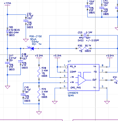
Good afternoon, I am using the subject amplifier in a transimpedance application  with a photodiode. Currently, in addition to the transmipedace stage, we have a second gain stage and then a third stage with a VGA. We are trying to get rid of the second and third stages to combine the variable gain function into the transimpedance stage by using a device such as the TSA3357 part or similiar. See attached...

I am hoping to use the switch to bring in various feedback resistors in to modify the gain. I'm concerned about capacitance affecting the BW of the opamp. What else should I be concerned about? Are there other TI switches that would work better?

Thanks,

Robert

  • Hi Robert,

    You are absolutely correct that the main concern is going to be the switch capacitance. Unfortunately most external switches have too much capacitance for transimpedance designs in the frequency ranges of the LMH6629. The added capacitance will either limit the bandwidth or potentially make the amplifier unstable.

    On option may be to look at our OPA857. That part is a dedicated transimpedance amplifier with internally switchable 5k and 20k gain settings at over 100 MHz closed loop bandwidth. The internal switches avoid the issues with using an external part.

    Regards,
  • Jacob,

    Thanks for your prompt reply! I will review the datasheet the OPA857 part. Concerning the TSA3357 switch, the specs for capacitance of the common and NO contacts in reference to ground as shown in Figure 15. Correct me if I am wrong, but it seems like this capacitance may be an issue with signal distortiion, but not necessary BW? I was looking for a spec in the datasheet for a spec for the capacitance across the switch (from the NO contact to Common), which would seem to affect BW more? 

    Thanks!

    Robert

  • Hi Robert,

    I can't find a datasheet for the switches you reference, but the capacitance becomes an issue in the stability and bandwidth response of the amplifier. The high frequency gain of a transimpedance amplifier is set by the input capacitance (usually dominated by the diode) divided by the feedback capacitance. This can cause a stability problem if the high frequency gain is less than the minimum stable gain of the amplifier. The closed loop transimpedance bandwidth is also effected by both the feedback resistor and capacitances. Typically high frequency switch capacitances in the feedback loop can alter the high frequency response and cause the amplifier to become unstable.

    Below is a link to one of our app notes that explains high speed transimpedance in detail.
    www.ti.com/.../sboa122.pdf

    Regards,
    Jacob
  • Jacob,

    The switch PN is actually TS5A3357, sorry for the confusion. My question is concerning the switch specifications on capacitance. The capacitance specs appear to be given in reference to ground for the terminals of the switch. I am curious about any parasitic capacitance across the NO and COM terminals. There is no spec for that in the datasheet, but if you look at the spice file, it appears to be 1.47pF? Could you confirm this? Also, am I correct in assuming that the capacitance to ground is more of a stability issue, whereas parasitic capacitance across the switch terminals would do more to reduce the BW?

    Thanks!

    Robert 

  • Hi Robert,

    The series capacitance shouldn't be too much of an issue as long as you always have some resistance in series with the switch as well. You will also want to make sure you have just a normal restive path around the feedback as well so that there is no case where the amplifier can be open loop. It is possible that the switches will start to look close at high frequency and modulate your gain because of the series capacitance, but if it is only 1.4pF then it may not be an issue.

    The capacitances to ground will be more of an issue. If possible I would add some output isolation resistance directly on the amplifier's output (10 ohms would be a good start) and then connect the switch(es) after the series output resistor. You definitely do not want to connect the switches on the input side because the extra capacitance will likely make the amplifier oscillate. The output is still also susceptible to the capacitance, but can handle a bit more and the isolation resistor will help to take care of it at the sacrifice of some output headroom.

    I would suggest trying some of these simulations using the LMH6629 TINA-TI model.

    Regards,
  • Hey Jacob,

    I will keep these suggestions in mind for this design. Thanks for the feedback!

    Robert