This thread has been locked.

If you have a related question, please click the "Ask a related question" button in the top right corner. The newly created question will be automatically linked to this question.

INA125: Bad data captured from adc

Part Number: INA125
Other Parts Discussed in Thread: LM317

Hi to all! 

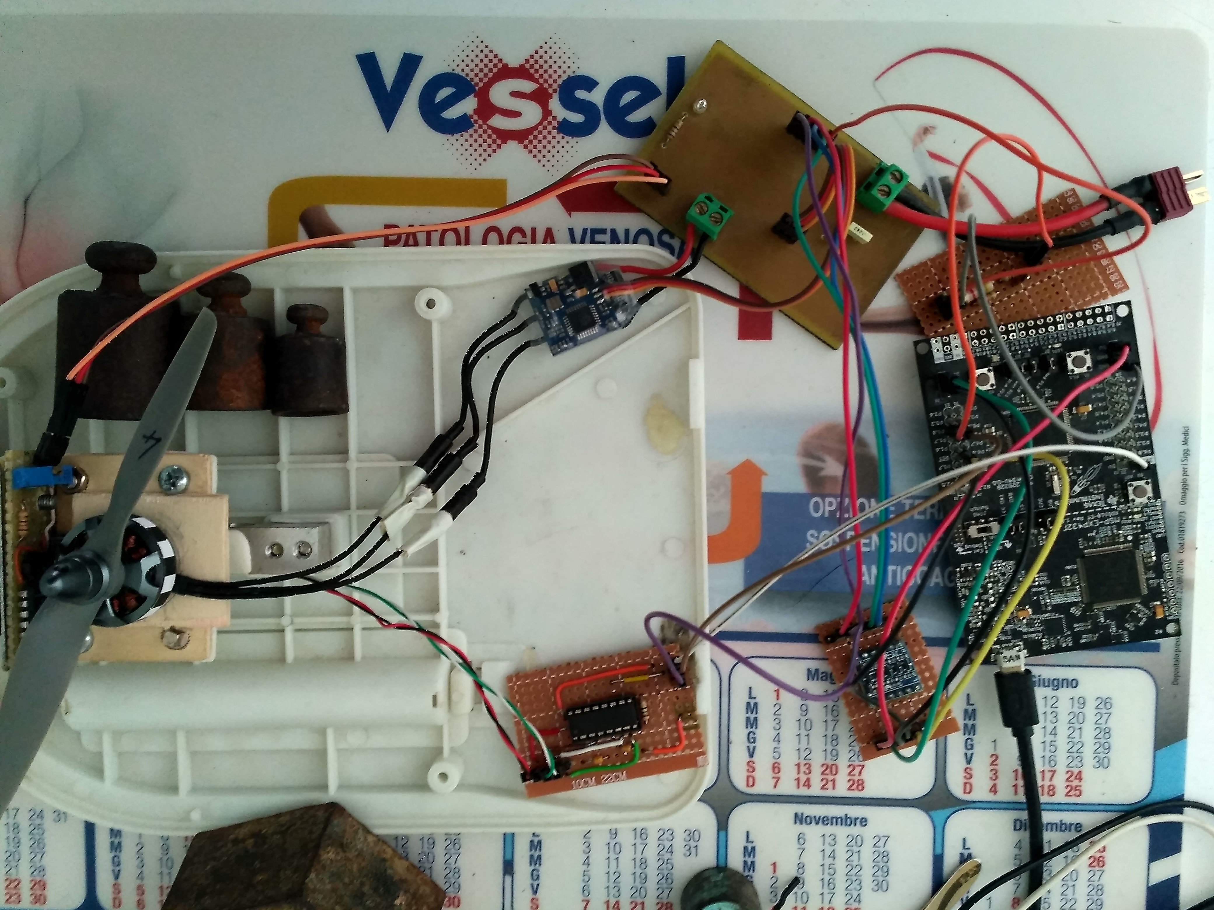
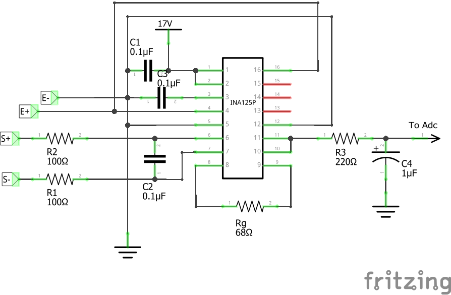
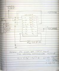
I have a problem to acquire the output signal from the INA125P. My circuit is like to this (from forum.43oh.com/.../):

the only difference is that i have added a 0.1uF capacitor between S+ and S-. This work fine if I use it for the normal weighting operation, but work bad if i need to measure a thrust from a bldc motor with propeller.

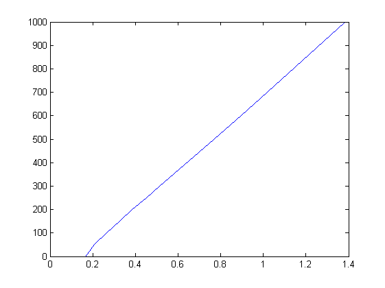
In particular during an acquisition session i obtain this signal from adc:

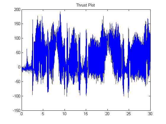
this is very noisy and unuseful signal because this signal have much negative values, so i can't use it for my purpose.

However i have tryed to insert a RC filter and i obtained some improvement:

I obtained this signal using the original circuit above ( without the 0.1uF capacitor between S+ and S- ) and a RC circuit whit R = 4.7KOhm and C = 4.7uF. I have used this value because with other values i obtain however some negative values. However this signal is less usefull because i can't measure the full thrust generated of my motor and propeller. I understand that this is due from the RC filter that isn't fast, but i not know how to improve this signal using a different value of R and C without have a negative value.

My question is, how i can improve the circuit to obtain a better and usable signal for my purpose? I'm not an electrical engineering, so i have some problem to find a solution.

  • Hi Luca,

    The small INA125 circuit is not legible and we are unable to make out the circuit details. I realize it wasn't legible on the website, but could you please provide a more view-able circuit diagram? We need to see the details.

    Please provide information about the motor that drives the propeller. Is it a PWM or another type of motor? How physically close is the motor to the sensor bridge? What precautions were taken to assure that the INA125 circuit doesn't have noise from the motor and surroundings induced into it?

    What does the INA125 output look like when the motor is turned off?

    Can you provide a photo of your measurement setup?

    Regards, Thomas
    Precision Amplifiers Applications Engineering
  • Hi Thomas, thank you so much for the reply!

    I'm sorry for the bad image, however this is the INA125P circuit:

    I used this for acquiring the signal in the first image. The signal in the second image is acquired with this circuit without the C2 capacitor and plus whit a RC filter in output with R = 4.7 Ohm and C = 4.7 uF.

    The motor is a BLDC, it is drived by an ESC. The motor is on the edge of the load cell, it is  a few cm above the load cell. At this moment i haven't nothing precaution about induced noise. This is a photo of my setup:

    When the motor is off (like the photo above), i measure a 0.21 V on the INA125P output pin.

  • Hi Luca,

    Thank you for all the additional information about your INA125 application. I have reviewed your circuit design and have concerns about the implementation:

    • The INA125 is set for a gain of 4000 V/V; that is a very, very high gain. Not only will the differential voltage from the bridge be amplified by this gain, but all noise picked up by the interconnect wires and circuitry. The photos that you ave provided show tremendous amplification of noise riding on input bridge voltages. Circuits operating with such high gain must be enclosed in metal enclosures and connections to the bridge must use shielded cables.
    • The INA125 is only powered by a single, +3.3 V supply in your circuit. That much limits the voltage range that can be applied to the VIN+ and VIN- pins. There isn't a datasheet plot for the input common-mode voltage (VCM) range for a single +3.3 V supply, but the INPUT COMMON-MODE VOLTAGE vs OUTPUT VOLTAGE, VS = ±5V plot on Pg 5, shows the VCM range for a single + 5 V supply. That plot indicates that the minimum VCM is about +0.75 V, and in your circuit the voltage at the VIN+ and VIN- inputs is about +0.625 V because the bridge bias voltage is only +1.25 V (pin 13). This assumes all 4 resistors in the bridge are equal value. Very likely, you are attempting to operate the INA125 below its minimum VCM capability.
    • The very high 4000 V/V gain also amplifies the voltage offset (Vos) of the INA125. The specified input referred Vos is +/-75 uV typical, +/-500 uV maximum, with a +5 V supply and at room temperature. It might actually be higher with a +3.3 V supply. If you multiply to typical and maximum input Vos levels by 4000 V/V, the output referred voltage offset Voso would be +/-0.3 V and +/2 V, respectively. This Voso will add, or subtract from the expected output voltage resulting from the bridge operation. Keep in mind that the INA125 output with Vs = +5 V is limited to (V+) - 1.2 V on the high end, and (V-) + 0.3 V on the low end. Applying these limits to Vs = + 3.3 V at best the high level output swing limit will be about +2.1 V, and about +0.3 V on the low end, for an output voltage swing range of 1.7 Vpp. You can see that the amplified voltage-offset Voso is huge in comparison to the available output swing range.
    • In general, it appears that more consideration needs to be given to the way the INA125 is being applied.  I suspect that the negative noise spikes that drop below 0 V are due to fields being generated by the motor and is being coupled through the circuit. The INA125 operated from a single +3.3 V supply is not capable of driving its output below 0 V.

    Some suggestions for improving the circuit:

    • Increase the supply voltage to a higher level if possible. That will increase the output swing range and allow you to use a higher reference voltage than the current +1.25 V. Raising the reference voltage applied to the bridge increases the VCM voltage applied to the INA125 inputs and moves it away from the bottom end of the range.
    • Mount all of the circuitry inside a metal enclosure. Make sure any connections to the bridge use shielded cables.
    • Consider reducing the gain of the INA125 and follow it with a gain stage. That gain stage could be configured as an active filter to help reduce high frequency noise.
    • If you have access to an electrical engineer they may be able to help you resolve the issues with this application.

    Regards, Thomas

    Precision Amplifiers Applications Engineering

  • Hi Thomas, thank again for the reply!
    At first read, I intuit what you tell me, now i try to re-read and understand better your answer and after i try to do what you tell me!
    However i have to tell you an important thing about the graphs above. It's my mistake that i don't have specifing this before, i'm sorry. The graphs above in reality are a bit elaborate, they represent the values in gramms and not in volt.
    When i acquire the signal from the load cell, before start the motor, i acquire some samples and afert i do the mean of they. This represent the tare of my rotor (motor+propellers+support). After this operation, I give a reference signal to the motor and i acquire the signals from load cell. When the acquisition finish i remove from this value the tare and i convert the result in gramms. The negative value are due to this software operation. Tomorrow i post a graph with a non elaborate values, however i think that this values aren't negative.

    I have two other question about your answer:
    what you means when you tell me that "Make sure any connections to the bridge use shielded cables."? I can't have access to the strain gauge of the load cell whitout broken it.

    I have another "version" of the INA125P shield, in this version i use an LM317 to supply the voltage of the INA125. The output of the LM317 is set to about 7V. In this case the max output of the INA125 is below the 5V but this is an hight voltage for the MSP432 ADC. The MSP432 ADC work on the 3.3V. I have tryed to create a voltage divider to lower the output, but i doesn't had success because i don't able to find in the datasheet the max output current of the INA125. Can you suggest me a value of the max output current of INA125 so i can implement an voltage divider?
  • Hi Luca,

    Regarding your questions:

    1) What you means when you tell me that "Make sure any connections to the bridge use shielded cables."? I can't have access to the strain gauge of the load cell whitout broken it.

    My concern is that noise picked up by the wires going to the bridge is amplified by the very high INA125 gain. This noise will modulate the dc levels that are established by the bridge in response to the load. Some of the fast output variation of the INA125 is certainly from the bridge reacting to the propoller as it turns, but I expect there is noise pick up at the input as well. Noise introduces error in the output and the goal is almost always to only amplify the intended input signal.

    If the the individual wires from the motor can't be shielded, it may be possible to place them together in a shielded metal braid. Another possibility is twisting the two wires that attach to the IN+ and IN- together, and then twisting the bridge bias from VREF and the ground line together. Essentially, these create two twisted-pairs that provide a degree of common-mode noise immunity. It should be better than having the wires openly exposed to the noise environment.

    2) I have another "version" of the INA125P shield, in this version i use an LM317 to supply the voltage of the INA125. The output of the LM317 is set to about 7V. In this case the max output of the INA125 is below the 5V but this is an hight voltage for the MSP432 ADC. The MSP432 ADC work on the 3.3V. I have tryed to create a voltage divider to lower the output, but i doesn't had success because i don't able to find in the datasheet the max output current of the INA125. Can you suggest me a value of the max output current of INA125 so i can implement an voltage divider?

    The +7 V Vs level is preferable to the +3.3 V level because it gives you more options for the VREF level. The INA125 isn't capable of driving a lot of output current. Most of the datasheet soutput specifications are written using a 10 kΩ load resistance. If you set up a resistive divider make sure that the total resistance is around 10 kΩ. Be aware that the INA125 output voltage range does not swing down to 0 V, or up to the Vs+ rail when a single supply is used. If you want to achieve an output voltage that goes to 0 V, then the INA125 would have to be powered off dual polarity supplies such as +/-5 V, etc.

    Note that most ADCs require the correct interface between the amplifier that drives them and their input. Otherwise, their true resolution may not be realized. Unless the ADC input is internally buffered that usually requires using an op amp with the necessary current output drive capability and a carefully determined RC network. This in itself can prove to be quite the engineering task.

    Regards, Thomas

    Precision Amplifiers Applications Engineering

  • Hi Thomas,
    I realize that this is a difficult task for me, but i'm not know a friend that is an electrical engineer, so i try to solve my self this problem..
    In reality, after reading the MSP432 datasheet, i have started to play with the RC filter. For my adc setup an RC filter with R=4.7KOhm and C=22pF is a right chooses, but with this filter i obtain a very bad signal, so i have asked in this forum..
    Regarding the shielded cable, i have twisted the IN+ and IN- and the Vref and Ground togheter, you can see the result in the photo above, however tomorrow i try to implement some shielded metal braid for this cable, also i try to find a metal box to enclose te entire circuit.

    I have another question about the circuit:
    Have sense to use some decoupling capacitor in this circuit? Also I have see on internet some circuit with the INA125 that use an input filter on IN+ and IN-, this may help to reduce the induced noise? In the positive case, can you suggest me some values for the resistor and capacitor?
  • Hi Luca,

    Well, it is admirable that you have made this much progress putting the system electronics together when electronics it is not your specialization!

    Regarding your question:

    Have sense to use some decoupling capacitor in this circuit? Also I have see on internet some circuit with the INA125 that use an input filter on IN+ and IN-, this may help to reduce the induced noise? In the positive case, can you suggest me some values for the resistor and capacitor?

    It is a common practice to include a common-mode, differential-mode at the inputs of an instrumentation amplifier (INA). Limiting the bandwidth of the system with an input filter will result in less noise at the IA output, compared to when the full bandwidth of the system is allowed.

    We would need to know the frequency range that must be supported, before any filter component suggestions can be suggested. If the ability to measure a slow dc change is all that is needed, the filter cutoff frequency can be very low. However, if the specific frequencies associated the propeler speed must pass through the amplifier, then the cutoff frequency must be much higher.

    Regards, Thomas

    Precision Amplifiers Applications Engineering

  • Hi Thomas,

    I appreciate your words, they make me very happy, thanks you so much! ;)

    However after a day of experiment, now i have some result. I have used the version with Vs = 7V and Vref = 5V. In practice with this setup, if I use a different gain (Rg = 120, 100, 82 Ohm) I obtain a characteristic that is non linear with low weight. Also seem that the signal is a bit better than the signal with the old setup. But i have spend more time to understand why the non linearity come out, so i haven't used any precaution about the noise. Tomorrow i do more experiments using the precauctions for the noise (ie shielded cable, input filter and decoupling capacitor). 

    I have to ask a question. in your opinion, is better if i use the pseudograund circuit to elimintate the nonlinearity and the problem about noise?

  • Hi Luca,

    The INA125 should be highly linear if operated within the specified, linear input VCM and output swing ranges; even over a small input range. Check the linearity specifications of the bridge. By the way, what are the resistances of the bridge resistors?

    FIGURE 6, Psuedoground Bridge Measurement, 5V Single Supply, states “Psuedoground” is at +2.5V above actual ground. This provides a precision reference voltage for succeeding single-supply op amp stages." Using the psuedoground is a convenient way to provide a low-impedance +2.5 V reference for the op amp stages that follow the INA125. For example, if those stages use a V+ level of 5 V this places their VCM right between ground and V+. Their mid-level output level will be centered for maximum plus and minus swing.

    The pseudoground is not intended to be the system ground. The chassis ground, or common, should serve as the system ground for the bridge and the circuits. It should provide the lowest impedance path to the return currents.

    Regards, Thomas
    Precision Amplifiers Applications Engineering
  • Hi Thomas,

    I have changed my circuit, now it is this:

    However the result doesn't change, i obtain this signal from last acquisition:

    in this case, the value are in volt. When acquire this signal, i don't any operation for subtract the tare. 

    For the nonlinearity, after some experiment I realized that if I increase the Vs and if I reduce the Rg value, the nonlinearity disappear, this is that I get using the circuit above:

    However if i use a 12V supply voltage, with the same circuit I obtain this characteristic:

    If i increase the Rg value (82, 100, 120 etc..) or if i decrease the supply voltage, the non linearity i more accentuated.

    After read your last post, i have some doubt about the correct operation of the INA125, maybe i have broken it. If I use a 17V for supply the INA125, the output of pin 16 isn't 10V but it is 12.76V and the Vcm is 6.38V. The same appear if I use a 12V for the supply, the output for the pin 16 is 9.18V and the Vcm is 4.59V.

    I have measured the load cell resistance that is about 994 Ohm between E+ and E-, and 746 Ohm between S+(S-) and E+(E-).

    Note that i have used an protection for the load cell cable, like a aluminium paper that i found in a broken TV scart cable.

  • Hi Luca,

    Increasing the INA125 supply voltage should work to your advantage by extending the VCM range, increasing the VREF selection options and increasing the output voltage swing range. Those should al be good things.

    INA125 pins 12 through 15 are open which would wire the refernce amp for an output of +10 V. That is the voltage that would appear at Pin 4, the VREFOUT point, and that voltage would be applied across the total bridge resistance. When the bridge is balanced the S+ and S- levels should be at half that, or +5 V each (providing it is a balanced bridge with all Rs being equal). If you are not measuring those values your INA125 may be in trouble.

    I am not quite sure about the bridge resistances you are measuring. If you have the INA125 in the circuit with the bridge attached you may be getting some other resistances mixed in with your intended measurement. Despite this, it looks like the resistance presented to the VREFOUT may be less than 1000 ohms, in which case the current demand may be too high for that reference op amp to deliver. The INA125 datasheet on Pg. 12 mentions, "Output drive capability of the voltage reference is improved by connecting a transistor as shown in Figure 4. The external transistor also serves to remove power from the INA125." The transistor probably doesn't need to be as current capable as a TIP29, but just something that can readily provide tens of milliamperes.

    The horizontal scales are labled in the graphs. If they represent output voltage it may be the output is being driven into the lower output swing range limit. Increasing the INA125 gain would result in the output attempting to swing over a greater range and would hit the rail where the linearity would appear to be worse. Backing off on the gain and keeping the output away from the rails should improve output linearity.

    Once you get the INA125 circuit operating well from a dc standpoint I can provide some suggestions for adding differential and common-mode filtering right at the INA125 inputs. Currently, you have a differential-mode input filter consisting of R1, R2 and C2, and another at the INA125 output R3, C4. Very often noise is common-mode in nature and can be the real problem.

    Regards, Thomas

    Precision Amplifiers Applications Engineering

  • Hi Thomas,

    I confirm that if Vs is 17.04V, the VREFOUT at pin 4 is 12,78V and the voltage at pin 6 is 6.40V and the voltage at pin 7 is 6.40V. I have done this measure with the load cell attached to the INA125. With the load cel disconected I measure this value of 16.30V at pin 4. 

    Is my INA125 broken?

    Also i confirm that the resistance between E+ and E- of the load cell is 994 Ohm, measured with the load cell disconected from the circuit. The voltage between S+ and E+ and the other combinations of they is 746Ohm. I can using any type of NPN transitor? The C945 is good?

    Ps

    For the input/output filter, I'm referring to the "Analog Engineer Calculator" tool from TI. For the input filter I have used a circuit that i found in the section "Amplifier and Comparators". Follows your answer, i realize that the correct circuit is this:

    or i'm wrong? 

    I haven't idea how to change the output filter. I follow the same circuit of this tool ithat i found in the section "Passive" -> "RC Low Pass Filter". 

  • Hi Luca,

    The VREF voltage is established by the bandgap and that is amplified by the reference amplifier gain setting. Your circuit is set up for a VREF voltage of +10 V and that is what it should be unless the VREFOUT is being pulled down by an excessively high current load. However, in your case the VREFOUT is higher than it should be. That tends to suggest that your INA125 is damaged. 

    A load of 994 Ohms with a  proper 10 V VREFOUT is over 10 mA, which is too much for the INA125. It should have the driver transistor added. I would select an NPN transistor that is rated for 200 mA, or more, and can handle the power dissipation. 

    Do realize that the Vo in your circuit design is referenced to 0 V, which means the output will be driven into the rail when the bridge response tries to drive the output downward. It is important that you use the Psuedground bridge circuit shown in datasheet Figure 6 - even with your 17 V supply. Select the VREF level that is most compatible with your application needs and then set up the tap on the VREF resistor string. For example for IAREF to be set to 5 V, pin 4 is connected to Pin 15, and a wire is connected from them to the IAREF pin 5. Then as the resistance changes VOUT will move up or down relative to +5 V.

    I built an approximate TINA model of the INA125 and simulated the psueudoground pin biased at +5 V. The circuit functions as expected. The gain is very high and a 10 Ohm change in any one of the bridge resistors moves the output a couple of volts. Note that I had to use 5 K resistors in the bridge because the op amps I used in the model couldn't drive 1 k resistors. Again, the need for the bridge buffer transistor is verified.

    The filter scheme shown for the instrumentation amplifier circuit shown above is only effective for common-mode noise, but that is often the most troubling kind. It is imperative that for best filter performance RIN1 and RIN2, and CCM1 and CCM2, be closely matched in value. If they are mismatched the common-mode noise will be partially converted to differential-mode noise, which will be amplified by the amplifier's differential gain. Differential-mode filtering can be added by bridging a capacitor across from CCM1 and CCM2

    This particular INA125 topic has been requiring a goodly amount of time to support. We need to bring this to resolution soon as there is a limit to the service we can provide.

    Regards, Thomas

    Precision Amplifiers Applications Engineering

    INA125_Sngl_Sply_02.TSC

  • Hi Thomas,

    If my INA125 is damaged, I think that other words about it are useless! I have ordered another INA125, when I have it on my hand I try to apply all advice that you given me.

    For now, i mark your last post as solution, thank you so much for all your support.

    Best Regards

  • Hi Luca,

    I think you have enough information now to get your INA125 circuit working. Noise pick up will probably be your biggest issue moving forward. One you have the entire assembly enclosed in a metal enclosure that should help a lot.

    I am going to go ahead and close this E2E inquiry for now. If you find you have some additional questions you can reopen this inquiry, or start a new one.

    Good luck with your INA125 circuit!

    Regards, Thomas

    Precision Amplifiers Applications Engineering