

Other Parts Discussed in Thread: INA193
How to understand the bandwidth specification and how it applies in relation to my PWM control signal

This thread has been locked.
If you have a related question, please click the "Ask a related question" button in the top right corner. The newly created question will be automatically linked to this question.
The INA240 employs a novel architecture similar to traditional chopper stabilized amplifier, with the main objective to minimize low frequency error and drift, while enabling inline current sensing in a PWM environment. As a result, INA240 exhibits excellent PWM rejection, DC accuracy and temperature drift.
There are occasional questions when it comes to understanding the relationship among the following parameters:
This post will try to shed some light on each of these areas.
1. PWM Frequency and Duty Cycle
In BLDC motor control, the winding current needs to be monitored cycle by cycle. The quicker the current sense amplifier settles after a PWM transition, the faster the controller can make a decision based on the current measurement. Two parameters of the PWM immediately come into picture, namely, (1) PWM frequency and (2) PWM duty cycle.
Sometimes one would ask, why can’t I use a current shunt monitor (CSM) that has a bandwidth of 100KHz, for a 100KHz PWM application? It is not a simple yes/no answer, instead, it depends on the accuracy requirement and settling time in relation to the frequency and duty cycle of the PWM signal involved.
Using the same 100KHz PWM example, let’s assume its duty cycle is 50%. After each PWM transition, the current normally changes and therefore the CSM has to settle to the new differential input. The CSM is really being provided with an input signal that has a fundamental frequency of 200KHz. To the maximum, the CSM has 5uS to work with, instead of 10uS, before the next measurement has to take place. During the 5uS, the CSM has to amplify the differential input, while settle out the common mode disturbances.
The situation can be even more challenging when the duty cycle is varying. Take the same 100KHz PWM signal, if the duty cycle is 25%, then the workable time reduces from 5uS to 2.5uS.
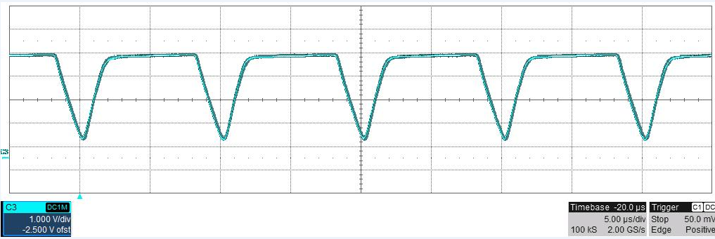
To illustrate the effect of duty cycle, a 100KHz differential input, with two different duty cycles are passed to the same CSM, the response diagrams are shown below. Even though in reality the differential input presented to the CSM by a motor is rarely square wave.
 |
| Figure 1 Step response, 100KHz and 20% duty cycle |
 |
|
Figure 2 Step response, 100KHz and 80% duty cycle |
2. INA240 Bandwidth (-3dB frequency)
The Band Width (BW) is defined as the half-power point, ie, the frequency at which the output power drops to half of its peak. It is also referred to as -3dB frequency.
INA240 has a relatively high slew rate of 2V/uS; and relatively wide bandwidth of 400KHz. THDN is about 2% at 100 KHz, and increases rapidly at the higher portion of the bandwidth, as evident from the following figure.
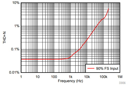 |
| Figure 3 INA240 THDN curve |
The following is a time domain plot of a 400KHz sine input, being amplified by INA240A1. The output still has half the peak power but the waveform begins to look more triangular than sinusoidal.
 |
| Figure 4 INA240 response to 400KHz sine input |
3. INA240 Settling Time
In the INA240 Electrical Characteristics table, the settling time is shown as typically 9.6uS for 0.5% accuracy; this was tested with a 2V output step.
The settling time can be significantly shortened if the accuracy requirement is relaxed. For example, the settling time is typically 5uS for 1% accuracy.
The INA240 employs a unique offset cancellation topology to achieve exceptional PWM common mode rejection, and exceptional DC accuracy. This comes at the price of slower differential settling and larger distortion at higher frequencies.
Internally, the offset cancellation rans on a 400KHz(2.5uS period) clock. A change in differential input will need a few such clock cycles to be sampled and amplified. If the input is a slow with respect to this clock, the offset cancellation algorithm has to catch up with it all the time, at the speed of every 2.5uS.
This is why there are “steps” or “waves” in the response curves, as opposed to that of a traditional linear amplifier.
Obviously, this clock is asynchronous with respect to the input provided by the outside world; this is why the “steps” or “waves” will shift around depending on the relative timing of the input and the clock. The same offset cancellation scheme is also responsible for the distortion at higher frequencies
 |
|
Figure 5 INA240 differential step and ramp responses |
 |
| Figure 6 INA193 differential step and ramp responses |
Conclusion
The INA240 is specially designed for PWM applications, and is ideal for motor inline sensing. When considering INA240 for such applications, several parameters should be weighed to determine if it is a match. These parameters include the PWM frequency, duty cycle and settling requirement.
TI makes no warranties and assumes no liability for applications assistance or customer product design. You are fully responsible for all design decisions and engineering with regard to your products, including decisions relating to application of TI products. By providing technical information, TI does not intend to offer or provide engineering services or advice concerning your designs.
