This thread has been locked.

If you have a related question, please click the "Ask a related question" button in the top right corner. The newly created question will be automatically linked to this question.

LMH6629: Feedback pin causes input offset drift

Part Number: LMH6629
Other Parts Discussed in Thread: BUF634

For some requirements reasons, we have to use very low values for the feedback and gain resistors to build a simple amplifier using LMH6629, WSON8 package.

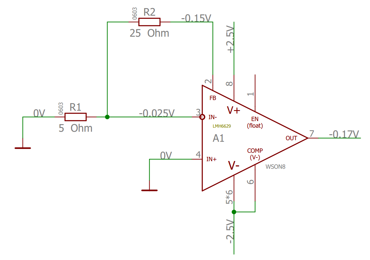
If we are connecting a feedback resistor R2 (25 Ohms, first attached picture) to the FB(Feedback) pin 2 of the LMH6629, the input offset voltage equivalent becomes in the range of 25...100 mV, depending on the R2 value and keeps changing.

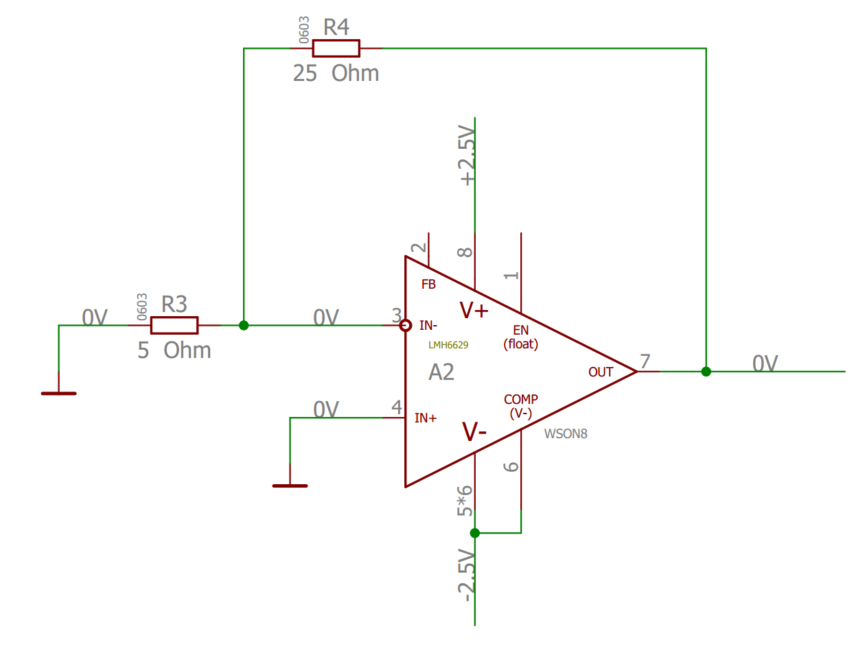
However, if we connect the same resistor to the OUT pin 7 directly, the amplifier works as expected (second attached picture).

Documentation also says that FB pin is Input/Output direction, while the OUT pin is output direction only.

Any potential issues if we will leave FB pin floating? It would be nice if we still could use FB pin instead of OUT pin to simplify PCB layout. 

Thanks!

  • Hi Hariton,

    hmm, 25mV input offset voltage? That's huge! Is your chip damaged?

    Kai
  • That was my first thought, too. I tried several boards, they are about the same. We have clamping diodes everywhere (not shown on the pictures) to protect from On/Off transitions. The only possibility for the chip to be damaged is by feedback resistor, which can create currents up to 100 mA. But the specified LMH6629 max linear current is +-250 mA, so it should not be the case, unless the feedback pin has a significantly lower max current. It may be true as we see on the picture 1 the drop voltage between OUT and FB pins of 20 mV.

    So I started from a fresh board with a feedback R2 resistor 100 Ohms. I saw a very slight offset. Then I started decreasing the R2 and the offset started increasing. When I put R2 back to 100 Ohms, it becomes back to normals.

    The largest offset that I saw was about 100mV with R2=10 Ohms, meaning load current 10 mA - this should not be a problem for the 250 mA capable chip.

    I know the 25 Ohms feedback resistor looks very unusual, to say at least, but we have to go that path. Our signals are about 1 mV, so loading the feedback should not be the issue.

    One thing that is not shown on the pictures is the input offset compensation voltage, that is about +10mV connected instead of the ground to the positive input pin, that we were planning to use to compensate normal +-1mV offset drifts, controlled by MCU. But our design gets saturated at about 15 mV and thats why I started wondering what could be a problem.
  • Hi Hariton,

    the input offset compensation scheme at the +input of LMH6629, could that cause the "offset voltage" of 5mV at the -input? Is this circuitry high ohmic?

    Is the output of LMH6629 free of oscillation?

    Kai
  • Hello Hariton,

    Check and see if it is oscillating at very high (>100MHz) frequencies. The "offset" you are seeing may be due to an oscillation. Is it getting hot? (more than normal?). Crank-up the time/div on the scope and look for >100MHz signals. You may need to eliminate any scope ground clips and ground the probe directly (or use the ground "springs").

    These ultra-wideband amps are sensitive to input impedance. The 30 ohm feedback resistance is *very* low. I assume you are using the extra low value feedback resistors to keep the noise and bias current effects low.

    If the input impedance is too low (<20 ohms), the input devices can self-oscillate at 100's of MHz. Section 7.3.3 gives a hint to this. Directly grounding the +IN, and/or the low value 5R gain set resistor, may be causing the input oscillations.

    Where are the "clamping diodes"? Diodes can add just enough capacitance in the wrong places to cause oscillations (and made worse by tricky varactor effects).

    The FB pin is bonded to the die, so the 'connection' between the output and FB pin is made through die metalization. This will have more resistance and inductance than if it were just a direct bond wire. So the "smaller" 30R value feedback resistor path is drawing 10x more current than the expected ~300R feedback resistance. So the extra current could be causing a voltage drop across the OUT->FB path.

    How *exactly* are you applying the offset compensation? The positive input pin is also sensitive to impedance and needs to see a certain impedance range.

    I know from experience with these GHz GBW devices that they are very picky about layout, bypassing and loading. The devices are optimized for a certain range of conditions and expected feedback component values and severely deviating from these can end in surprises...

    Check for oscillation whenever you see a large "offset"...
  • The +Input is connected through the 10 Ohm resistor to the ground. A 1k resistor from + input goes to the control circuit creating 100 times passive divider, so the +input is very low (10 Ohms) ohmic.

    Of course, we check for oscillations and yes, it is free from the oscillations. The design is done in accordance: shortest possible traces, ground plate removed around outputs, chip and -inputs, etc. Decoupling capacitors are reverse geometry low ESL plus tantalums, ferrite beads where required, etc. Power supply logs max currents and the chip never consumed more than 30 mA.

    Is FB pin capable of providing 250 mA current or it is only OUT pin?
  • I totally understand when you are saying to check for oscillations. This is the number one problem in many cases. I don't trust oscilloscopes much for such checks as they may create their own effects. First, we check for consuming currents. We have 100 Ohms passive load (in addition to the feedback pass), any oscillations will be visible by just checking the current. We have about 16 mA plus whatever the offset creates, so I am confident about it is free of them. We have a second stage that isolates the first (troubling) stage and I check with the oscilloscope the second stage output - there is only the normal noise levels. I have 1GHz oscilloscope.

    Clamping schottky diodes are for power supply pins, they are not connected to the inputs of the LMH6629. They protect from ground going above/below power supply rails. There are 0.5 pF clamping RF diodes at the later stages connected to the inputs, but that stages work fine.

    Section 7.3.3 and +input resistor: I think it is more about bias current cancellation (they advise to add a bypass capacitor to the +input). Just replaced 10 Ohms with 50 Ohms one: now we can compensate the offset within +-50 mV. Can't use the bypass cap here as it will create the phase shift in the divider. Other stages connect +inputs directly to the ground and they are ok.
  • Hello Hariton,

    In Section 7.3.3 , it mentions a minimum of 25 ohms... I can tell you from experience that this warning is real. These are VHF/UHF oscillations in the base of the input stage and may not be immediately noticeable at the output if the frequency is high enough. The oscillations usually manifests itself as a shifted DC offset or distorted output waveform (mixed products of any input signals). The amplitude can be very small, measured at the *input* pin , ~100mV or less. You can see this on a scope with the correct low-cap, high BW (FET) probes, but you have to know you are looking for a small, VHF/UHF signal on the *input* pins. It can be buried in the "fuzz" of modern GHz scope traces if you are not specifically looking for it.

    The Output pad and the FB pad are on opposite sides of the die and do not share any bond-wires or pads. My "educated guess" is the FB pin is not designed to handle the full currents of the output, which on a high-speed device, can be quite high due to the fast edge rates. That would require a BIG chunk of metal across the die. I figure there is about 4 ohms of resistance, so the metal traces are not that thick. Keep in mind that resistance is in series with your 25 ohms and affects the gain. Curious: Can you measure a resistance between FB and OUT?

    If you are probing the DC voltages with a DMM, try probing through a 10k resistor to isolate the DMM capacitance and prevent oscillations when probed. -25mV at the -IN pin is not correct, as the output should be railed full negative if that was the case. There should be less than 1mV measured *between* the +IN and -IN pins if it is functioning properly.

    Do the other stages use the same low value feedback resistors?

  • Hi Hariton,

    I agree with Paul. There can be oscillations in the input stage which might not result in an increased power supply current. Take care, the LMH6629 is no simple OPAmp which can be wired as desired. Too small feedback resistors can destabilize the input stage.

    Using a resistance of about 100...200R in series to the inputs can often be seen to stabilize the input stage of a HF-OPAmp. See section 8.1.1 of datasheet of BUF634. e.g. Usual feedback resistances are in the same order. If you now decrease the feedback resistances down to 5R/25R, this can be problematic. Resonances due to parasitic components are no longer damped and the input stage can oscillate.

    Kai
  • I have a hard time to understand: Section 7.3.3 and many other drawings (Figures 60, 64, 65, 66) suggest using bypass capacitors from +input to the ground, isn't it even worse than 10r, no-bypass input grounding? All our other stages connect +inputs to the ground directly with no problem, but they have 499 Ohms feedback resistors. I also tried to increase +input resistor but it didn't help other than increased offset compensation range to +-50 mV.

    Still, the main question remains: why FB pin causes the problem and OUT pin does not?

    My guess would be the relatively high resistance of the die creates voltage gradients that get picked up and amplified by the input stages of the LMH6629. This explains why offset is the accurate reverse proportion to the feedback resistor value, while oscillations do not explain it.

    It was a great idea to provide a dedicated FB pin, but unfortunately it was not implemented to support all possible uses and does cause noticeable input offsets (-25mV) that could otherwise be avoided.

    We will change the PCB design to connect feedback resistor to the OUT pin directly, or even run the airwire to avoid vias, I see this is as the only solution for us. We also hope in the future to see versions that would provide higher current capabilities in the FB pin.
  • Hi Hariton,

    I can understand that you are annoyed. But I think that the problem is not the FB pin but your excotic wiring of the chip. The LMH6629 wasn't designed for such low ohmic feedback resistances. Like Paul I'm pretty sure that the input stage is oscillating (provided the chip isn't damaged). An input offset voltage of 25mV is indicating that there's some terribly wrong with the circuit. And If the design is on the threshold of instability I don't think that it's a remedy to use the output pin instead of FB pin. The two output pins offer slight variations of parasitic components. That's the only reason why it seems to work with the output pin but not with the FB pin. But with a new batch of LMH6629 everything can change...

    Kai
  • Hi Hariton again,

    have you thought about adding a small resistance in series to the -input of LMH6629?

    Eventually the input stage oscillation can be stopped by this without eroding the phase margin too much?

    Kai