This thread has been locked.

If you have a related question, please click the "Ask a related question" button in the top right corner. The newly created question will be automatically linked to this question.

LMP7721: Gamma radiation sensor

Part Number: LMP7721
Other Parts Discussed in Thread: LMP7715

Hi all, 

I am modifying the circuit for a gamma radiation sensor used in our radio-synthesizer. Original design is attached. SOF-1861031106 - radAFERevG_HI.PDF As part of modification for noise and stability, I have decided to add a guard ring as recommended in the datasheet and LMP7721 multi-function evaluation board user's guide. In one part the datasheet states: "A cover or shield connected to the guard should protect the circuitry above (or below) the PC board". And in another part it says: "The guard trace should not be relied upon as the only method of shielding. A ground plane or shield should surround and protect the guard from large external leakages and noise, as the guard trace has the potential to couple noise back into the input".

As you can see on the schematic, there is a grounded shield that covers the whole circuit, and there is a second grounded shield that covers the PD which is mounted on the back of the board. Now the question is that;

1- Should I connect the main shield to the guard rind or shall I leave it connected to GND just the way it is?

2- Shall I connect the shield for PD to the guard ring or GND?

Thanks

  • Hello May,

    Never connect the guard to the main shield.

    The guard needs to surround the signal conductor. Think of the guard as insulation over a hot water pipe. The signal conductor should only "see" the guard trace surrounding it. The idea of the guard is to bleed off any external leakages across the insulation material (PCB).

    Connect the main shield to GND, as you have it. It is too far away from the traces and it will not make much difference. It would also act as a big antenna and inject noise into the guard system, making things worse.

    For the photo diode...it's a little different.

    Think of Triax cable: There is the center conductor carrying the "delicate" signal, the guard trace protecting the center conductor, and then the outer grounded braid shield that protects the guard trace.

    You want to build your circuit similarly - with the guard protecting the signal, then the shield protecting the guard from the environment.

    So for the photodiode, the guard should surround the immediate diode body. Then surround the whole diode "assembly" with a grounded shield.

    Since the diode is a 2-pin vertical right angle - I would place some copper tape around the sides and back (assuming reflections are not a problem) and tie it to the guard. Then surround the whole circuit with the shield.

    Since it is a thru-hole diode, don't forget about the pins sticking out of the bottom. The bottom anode pad should also have a guard ring and also a shield on the bottom of the board. Don't let outside noise "tickle" the diode's "feet" from below!

    Another option is to not thru-hole mount the diode but "surface mount" the diode by bending the leads and soldering to pads on the top layer only. Then below the diode you can pour a copper guard plane below the diode to minimize leakage through the PCB.
  • Hi May,

    I suggest you have a look at the LMP7721 EVM User's Guide that was composed by Paul Grohe, our LMP7721 "guru." He discusses Guards and Shields, in section 4.2.2. You can find the guide here:

    www.ti.com/.../snou004.pdf

    If that doesn't provide the information you need, let us know and we will try to assist you further.

    Regards, Thomas
    Precision Amplifiers Applications Engineering
  • Hi May,

    there's one critical issue with every photodiode, the optical window! In many applications the optical window stays open and presents a perfect antenna for interference. Even if you perfectly shield the rest of the TIA circuit, the unshielded die of photodiode itself always forms an electrode where electrical field lines of interference from outer world can easily end. This stray capacitance builds an entry port allowing charge being directly injected into the photodiode and by this into the signal path.

    A simple grounded metal netting can perform a surprisingly good shield for the optical window. Assume a metal netting which absorbs 10% of the light and allows 90% of the light to transmit, then this metal netting is able to shield more than 99% of the electrical field. The reason for this is, that electrical field lines are always searching for electrodes on which they can end. And when they find the metal netting, the very most of the field lines will end on it. Only the fraction of a fraction of the electrical field lines will pass the metal netting and end onto the die of photodiode.

    Where to connect this metal netting? To the guard? If it can be hit by ESD, then no. It's better to make the metal netting a part of the outer metal enclosure and connect both to signal ground.

    The grounded metal netting has also been discussed in this thread:

    e2e.ti.com/.../2656549

    e2e.ti.com/.../2659659

    Kai
  • Thank you Kai,

    I believe this should not be an issue for our design, since there is a grounded brass shield that goes around the photodiode, and is ultimately filled with black RTV silicone (this is block all light of course). But thanks for the suggestion.

    May

  • Hi Paul,

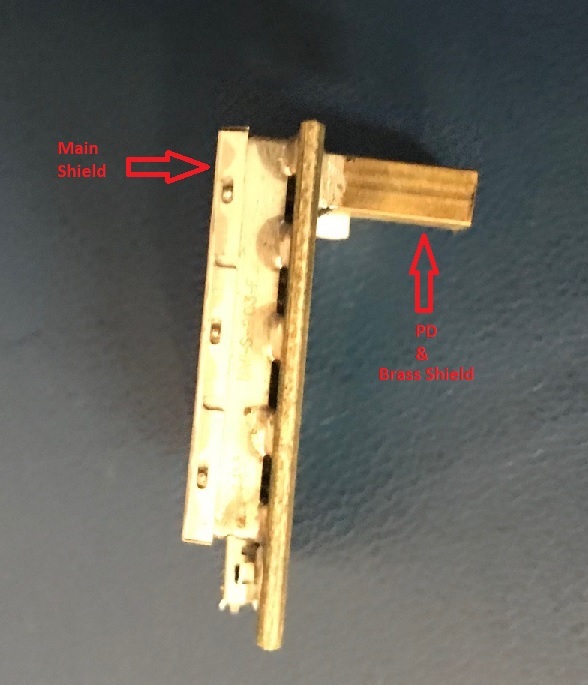
    Thanks for your detailed reply. So, the thru-hole PD is mounted on the back of the PCB and is encapsulated by a grounded brass shield. This means that the pins which stick out from the opposite side of the board, will be covered by the main shield. Is this enough or do I need to add more shielding? I have attached a photo from the side of the PCB showing how PD and it's shield are mounted in regards to the main circuit and shield.

    I am afraid I do not quite understand what you mean by "So for the photodiode, the guard should surround the immediate diode body. Then surround the whole diode "assembly" with a grounded shield." Do I need to wrap the diode first with grounded copper tape and then place the brass shield you mean? Or the brass shield in this case is sufficient?

    And as for the guard ring around Anode pad of PD; Do I need a ring on both sides of the PCB? I assume this ring can be connected to the main guard ring, right?

    Many Thanks,

    May

  • Hi May,

    The main shield is sufficient to cover the bottom of the pins.

    There should be a guard ring around the Anode pin on both sides of the board. It also helps to run vias between the top and bottom guard pads to create vertical guarding through the bulk cross-section of the PCB material.

    Ideally, you would wrap the copper tape around the diode, then tie the tape to the guard trace. The grounded brass shield would then surround the diode+copper tape guard.

    You mentioned encapsulating in silicone RTV. I have not done any studies - but it is possible that the RTV could generate charge when flexed. You may want to test for vibration sensitivity on one unit before potting all the boards. Ideally, the RTV should be on the "outer" side of the guard.

    Remember - the whole idea of a "guard" is to have a conductor of equal amplitude in parallel with the input conductor so that there is little to no voltage difference between the two conductors. So if there is a resistance (leakage) between the two conductors, no current flows since there is 0V difference, and any leakage from the "outside" world leaks into the low-impedance guard and is shunted away from the signal conductor.

    In your case, the input conductor sits at VREF_PRE, or about 418mV. If you had 1Gohm of leakage between the input and ground, you would see a constant 418pA current (418mV/1Gohm) . But if you add a second parallel conductor, driven to 400mV, now there should be no current flowing since there is no voltage difference (0V/1Gohm). The 418pA now "leaks" into the guard and not the input trace.

    So ideally you want to surround just the high impedance nodes with a guard (not the entire TIA circuit- only the input trace paths).
  • Hi Paul,

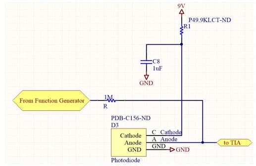
    I have questions about testing this circuit without the presence of Gamma radiation. I have been simulating input current pulses by running the output of a function generator through a large series resistor and tapping in the the IN- (pin8) of LMP7721, with the PD in place.

    Q1 - Is this a valid test?

    Q2 - If it is, then I want to add an SWG type connector to the same point (pin8) as a means of preliminary testing of these boards. So, when this connector is not being used, would it act like an antenna and impose noise into the input?

    Thanks,

    May

  • Hi May,

    By adding the DC coupled 1M resistor, you need to be aware that you will be turning it into a non-inverting amplifier for the signal generator path. -Rf/Rg= 10M/1M = -10. The input will be referenced to ground and not VREF.

    The non-inverting input (VREF) will also be gained up by the equivalent non-inverting gain (1+Rf/Rg =+11).

    The theoretical output will be the sum of the + and - paths, then gained-up by the "Tee"attenuation network.

    So it will be very important to get the DC offset of the generator to exactly match the VREF value as any error between the generator offset and VREF DC values will be amplified as offset.

    If you are using a AC signal or fast pulse, you can cap-couple the resistor to eliminate the DC matching issue.

    The correct way is to use integration to generate a known current.

    Remember:

    i = C * (dV/dt)

    If you have a known ramp rate, and known C, you can crate a known current. A triangle wave of a known amplitude will give you the delta-v and delta-t. A capacitor with a known, measured value gives you the C. You can play with the various dV, dt and C values to get the desired current.

    So you would replace the 1M resistor with a capacitor and drive with a triangle wave (not sine!).

    So if you had a 1V per second ramp into 1pF capacitor, you would get 1pA. As the input is ramping up (or down), you get a constant DC current.

    1pF * (1V/1s) = 1pF * (1) = 1pA

    Change the cap to 10pF, and you get 10pA

    Change the cap to 100pF, you get 100pA....1000pF gets 1000pA...you get the idea.

    Change the ramp rate to 10s and you get 100pA with 1000pF.

    Of course there is a finite time as you only have so much dV to utilize. But you can juggle the cap value and ramp rate. You can also scale it up into the AC range, but make sure the "triangle" is still linear.

    The cap should be large enough to swamp out any input capacitance. You can use a large cap, say 1000pF, but use small delta-V ramp by accurately attenuating the output of the generator into the 10's of mV.

    The SWG connector will add extra capacitance to the node. As long as you understand this, and correct for it, it should not be a problem as it is so small.
  • Hi May,

    is it for testing or calibrating?

    Kai
  • Hi Kai,
    This is for testing.
  • Hi May,

    I noticed that U2A and U4 are powered by different supplies. This can be dangerous for U4 during power-ups and power-downs or with the introduce of a testing scheme. I woud check the circuit whether U4 runs into latch-up when the output voltage of U2A exceeds the supply voltage of U4.

    If this issue is solved, I would use the following scheme:

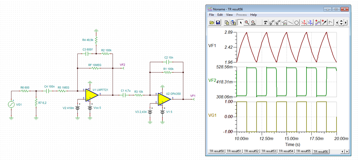
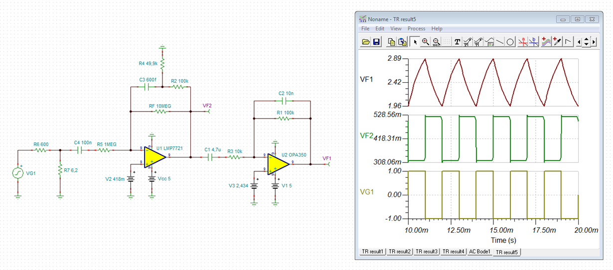
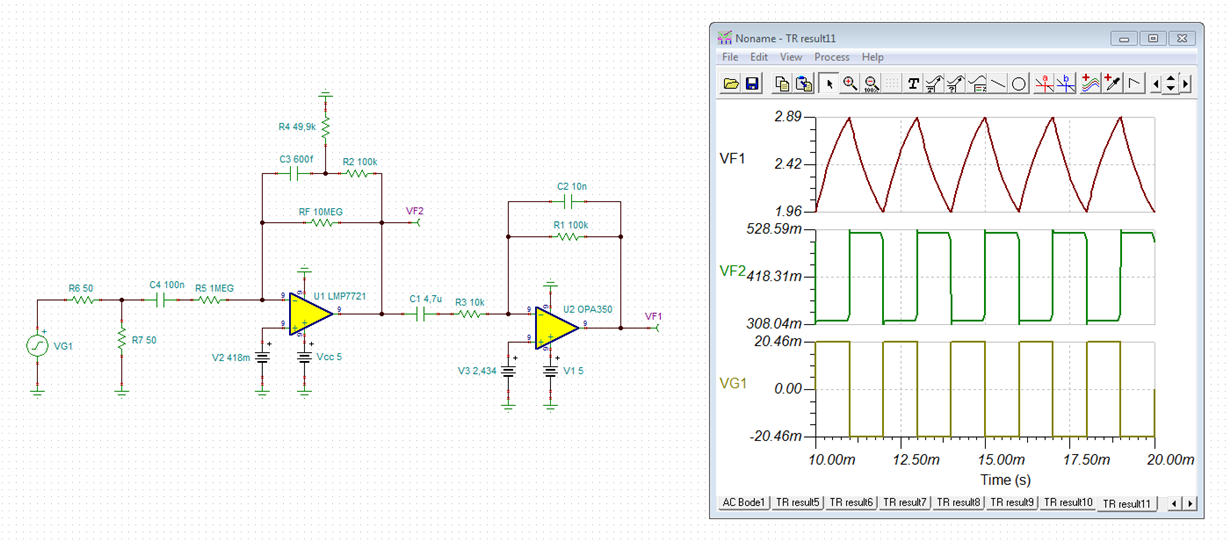
    A simple 500Hz square wave is used. R6 stands for the 600R output impedance many signal generators provide. R6 and R7 form a voltage divider. C4 is important to absorb the DC voltage difference between the signal generator and the virtual ground of OPAmp, as Paul already discussed. R5 translates the testing voltage into a testing current. A phase stability analysis has shown that U1 (in my circuit) will work stable with R5 at its input.

    Again, keep in mind, that it needs about one second before the operating point of the circuit has stabilized. During this time period the output of U2 (in my circuit) will hang in the posistive rail and will emit about 5V. If your comparator has a latch-up problem, this can be an issue.

    may.TSC

    Kai

  • Hi Kai,

    Thanks a lot for this detailed analysis. In fact I have no idea why the original designer has U4 on a separate power supply. As part of  design modifications I am removing U6 and connecting U2, U3 and U4, all to the same regulator (U1).

    You can see the changes I made so far in this file.

    RevH_test1.pdf

    As you can see I have also added a unity gain LMP7715 to drive the guard ring, and added the SG test circuitry.

    Originally I had planned to add a dedicated RC filter for LMP7721 power pins but I do not have the real estate on the board...

  • Hi May,

    maybe he wanted the comparator not making any switching noise on the supply voltage of LMP7721?

    Yes, I would also use RC filters in the supply lines, best for each OPAmp and the comparator. Even only a few Ohms can be very helpful.

    Kai

  • Hi May again,

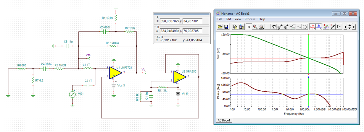
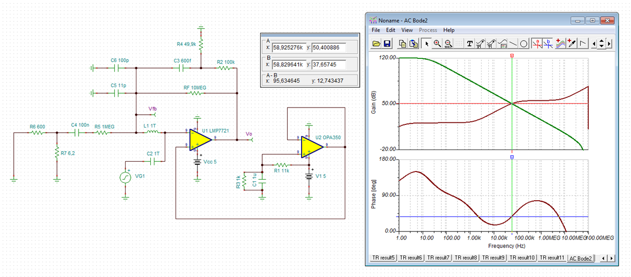
    I forgot to add the phase stability analysis:

    may1.TSC

    Kai

  • Hi May,

    If the guard does not extend off-board, and is completely within the grounded shield area, then you do not need a buffer. The "VREF" is already at low impedance (compared to the T-ohms if the input) and is sufficient to locally guard around the device.

    Just connect the guard to the VREF_Pre node (at U3, pin 12). That's it!

    The buffer was added to the EVAL board because the main connector is triaxial, and may need to be able to drive a triax cable (and possibly guard assemblies at the the input source at the end of the cable). That is too much to drive off of a simple resistor divider.

    There ! You saved some space!

    I would also recommend removing R14 and placing it in the test fixture. Then you eliminate a possible leakage path and extra capacitance (and possible cap soakage problems) through the R22, C24 & R14 node. Let that node float and surround all the node components with the guard.

    If *I* was going to do it... I would place *all* the "cal" components (R14, C24 & R22) on the "plug" side and just have the test connector on your board connected directly to the input. Then you would be calibrating all the boards with the same "cal" components instead of relying on the tolerances of the components on each board, giving you tighter board-board variation. You also save the space and cost of three components per board.

    If you *really* want to do it right, you would tie the shield of the connector to guard and guard up into the test fixture, then grab ground somewhere else (GND test point or screw). Otherwise, the test connector becomes a dominant source of leakage since the input pin "sees" ground and not guard. The connector had better have PTFE, or "Teflon" insulation and not plastic, in either case - so don't "cheap-out" on the connector.
  • I really appreciate the great support you guys provide!
    So, I removed the unity gain LMP7715 and connected the guard ring directly to VREF_PRE, also removed test network from the board as you recommended and connected the shield on test connector to guard. One question I have now is if a termination resistor is needed?
  • Hi May,

    The termination resistor, I assume is R14, is now in the "plug" end. That is good in that the high termination resistor currents are kept off-board.

    Are you really loading the generator down with 6.2 ohms? For most common generators, they expect a 50 ohm termination. With 6.2 ohms, the voltage across the termination resistor will not match the panel setting . I assume you are aware of this...
  • Hi May,

    the voltage divider setting with R6=600R and R7=6R2 is only an example. It allows to use a simple 2Vpp 500Hz square wave signal coming from a signal generator with 600R output impedance. You could even use a self-built 555-oscillator with a suited voltage divider. Or any other setup could be used to provide a signal of about 20mVpp at the left side of R5:

    Another issue: Removing the 1M resistor from the board is a bit critical, because the test cabling running to the -input of LMP7721 can introduce stray capacitance to this node then. This can erode the phase margin and cause instability. In the following phase stability analysis a stray capacitance of 100p is assumed which means a coax cable of about 1m length:

    So, if you remove the 1M resistor from the board, you must either use a very short cable or you must use the guarding technique Paul mentioned, which connects the cable shield of the testing cable to the guard and not to signal ground. By this, according to the general principle of guarding, the introduce of additional stray capacitance can be prevented or at least minimized.

    Kai

  • Hi Guys,

    Thanks a lot for all the details your provide.

    I have attached two schematics to give a better idea of what I am doing for the test fixture. The small test board provides test current pulses and power to main radiation sensor board.

    Test Board.pdf

    RADAFERevH_HI.pdf

    P2 on test board connects to P1 on sensor board through a short cable and the shield of both connectors is connected to the guard ring. As you can see, guard ring on test board encircles C1 and R2, shall I move R1 inside as well? Shall all of C1 be inside or only the side connected to R2?

    J2 on test board connects to U8 on sensor board and provides power and ground, also takes output of sensor board for measurements. Is this a good way of connecting GND between the two boards?

    Last but not least, individual RC filters for input power of U2, U3 and U4 on sensor board. LMP2271 datasheet recommends 100 ohm resistor and 100uF cap! 100uF caps usually come in larger packages, which could be a bottleneck. Would 10 or even 30uF be good enough? What do you suggest for the other two chips? Is 100 ohms and 1uF good enough?

    I really appreciate all your help.

    Thanks,

    May

  • Hi May,

    What is the frequency/pulse width of the test pulses?

    If the ground is through the USB cable, you will get some ringing. That is too much inductance. You should have a local ground near the J1 connector.

    Depending on space, you could place a ground "test point" near the J1 connector. Such as a single 0.1" header pin, and have a matching right-angle header socket on the cal board with the correct spacing so that both the J1 and GND pin mate when plugged-in.
  • Hi Paul,
    Frequency would be in the hundreds of KHz and duty cycle pretty short (1 or 2% max).
    That USB connector is actually going to change to a header type connector.

    Thanks,
    May
  • As long as the ground path is less than 1-2cm, then it should be okay.

    You want to ground the test jig as close to the photodiode circuit as possible. All in one header should be fine - just keep the analog (generator) and digital (USB) grounds separate until you get onto the board.
  • There is no digital ground. The board is not connected to USB, the connector is just used as a connector to take in power and ground and send out the output signal.There will be a power supply connected to J1 on test board. Part of the legacy of this design which will be changed.
  • Hi May,

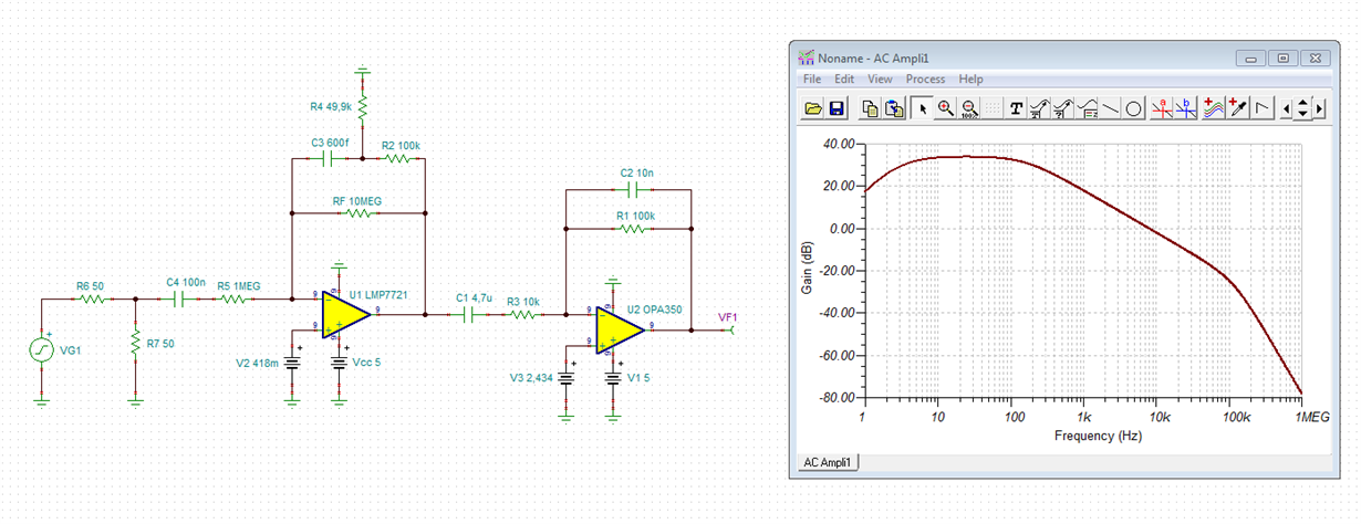
    the frequency repsonse of your circuit does not allow using a test signal with a frequency in the hundreds of kHz with a duty cycle of 1 or 2%:

    With such a test signal it's impossible to make the comparator toggle. That's why I have recommended using a square wave of 500Hz.

    Regarding the RC filter in the supply line: A 100R resistor makes only sense in combination with >=100µF. With a decoupling capacitance of only 1µF a resistor of 10...22R is better suited. Otherwise the impedance in the supply line could become too high.

    Kai

  •  Hello,

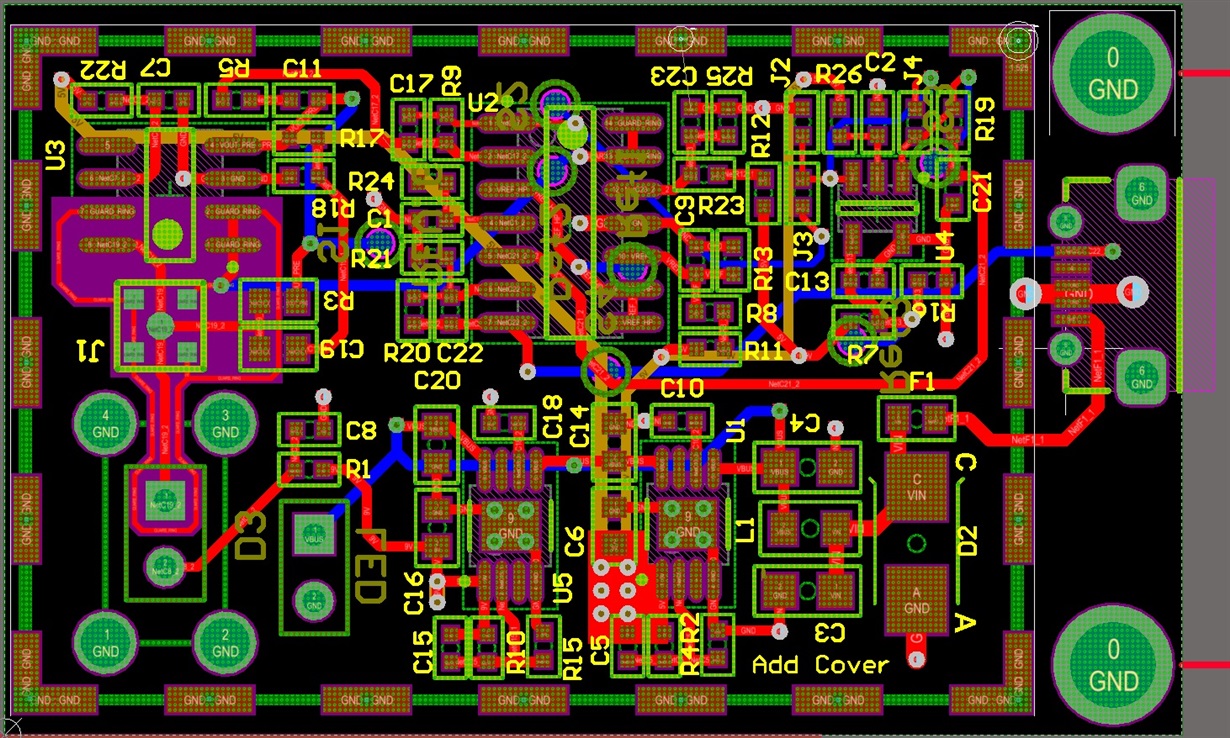
    May again! I almost completed the layout. Could you please take a look at the part containing LMP7721 (U3)? The purple polygon is top solder mask. There still remains one question for me though. Do I need to make the same polygon on bottom solder mask?

    Just to clarify;

    red -> top layer

    dark blue -> bottom layer

    light brown -> inner layer 2

    light blue (which is off) -> inner layer 1 (ground)

    Thanks,

    May

  • Hi Paul / Kai,

    I posted a screenshot of my layout, but I am not sure if you guys have seen it, since looks like I have replied to myself and not one of you. I would really appreciate if you could take a look and give me some feedback.

    I have the guard ring on top layer *red) and have removed the solder mask in that area (purple). I was just wondering if I need to do the same on the bottom layer or I can just fill the bottom layer with GND?

    red -> top layer

    dark blue -> bottom layer

    light brown -> inner layer 2

    light blue (which is off) -> inner layer 1 (ground)

    I really really appreciate your help.

    Thanks,

    May

  • Hi May,

    Sorry..I just got back from a business trip and I am still catching up..

    Yes. You want to guard both sides of the board around the input traces. Fill the bottom layer with a full guard plane under the active input circuitry. You do not need to remove the solder mask on the bottom layer.

    You want to surround the input circuitry with the guard, creating a guard "cocoon" around the input traces and components.

    Your impedance's are in the 10's of Megohms, so removing the solder mask from the top is not really necessary. Removing the solder mask is necessary when going to sub pA levels. The reason for removing the solder mask is to reduce surface charges - but you are not going to see that effect at your current sensitivity levels.

    The problem with removing the solder mask is that it exposes the bare FR4 to the ambient air (humidity). This can cause moisture to absorb into the FR4 over time, causing a long term drift (unless you add desiccant packs to the enclosure). I would just leave the solder mask in place to protect the board from moisture absorption (which will be much worse than any possible surface charge).
  • Hi Paul,
    Thank you for your response. Should I remove GND plain from underneath this part of the board on all inner layers as well?
  • Hi May,

    You only want to place the guard directly under the high impedance input circuity. If there are inner layers, place the guard plane on the layer directly below the input circuitry/traces. The layers below the guard can be "normal" layers.

    In short - the input traces should only "see" guard planes in all directions. The guard is "shielding" the input from the rest of the circuitry (even GND).

    Extending the guard under the "rest" of the circuitry increases the chances of noise pickup on the guard trace - so no need to guard the low impedance stuff...just put it under the input area.
  • May

    We haven't heard back from you, so we assume this answered your questions. If not just post another reply below.

    Thanks
    Dennis