Hallo,
I have a weird problem with the LOG114 log amplifier, which is the part of an experimental power supply for monitoring current consumption of low-power devices.
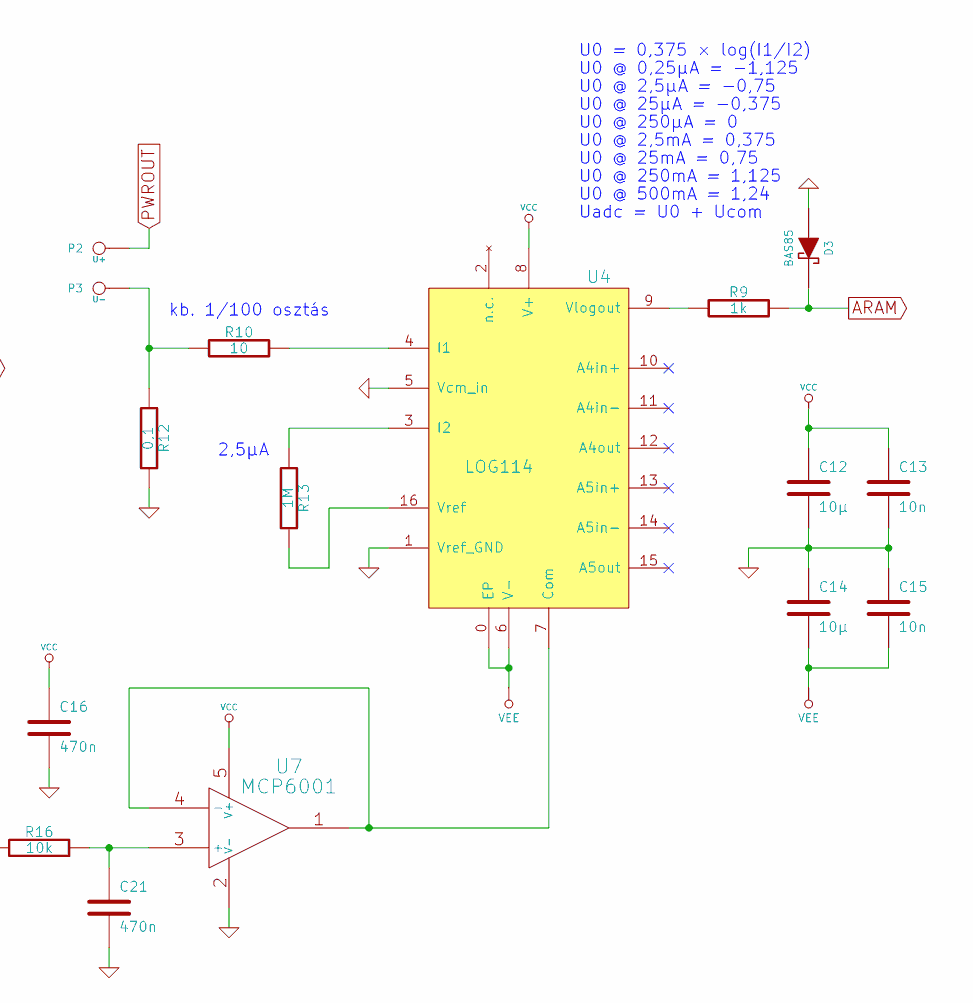
I include the relevant schematic part and the layout too.
Information to the schematic:
- The supply current of the DUT (powered by the circuit) is intended to flow from the P3 banana jack to GND (common ground plane designated with the triangle like ground symbol). The current is divided by R10 and R12, so approximately the hundredth of the current is expected to flow through the LOG114 I1 input to GND.
- VCC is +5V, VEE is –5V, supplied by 78L05 and 79L05 linear regulators.
- The Vcom is from a DAC buffered by U7.
- The "ARAM" reference label is connected to a single-ended ADC input (R9 and D3 protects the ADC from incidental negative voltages).
After the first power-up the Vlogout output of LOG114 was expected to be a negative voltage (to GND) with no current flowing in P3 (Vcom was set to 0V), but it was cca. +0.10V (to GND). This output voltage seemed to rise slowly until it reached cca. +0.3V. I tried multiple things:
- Tied P3 to GND. No change in the output.
- Connected P3 to a current source of a few tens of milliamperes. The output would be more positive, so something is working :)
- Resoldered the LOG114 many times. After soldering (but the circuit is still hot) the Vlogout pin went to near –5V, but during cool-down it was suddenly risen up to cca. –0.2V, and from this it was slowly increased to the original value.
- Cleaned the flux residues, no change.
- Connected the A4 and A5 internal op amps to a more fixed state (non-inverting input to GND, inverting input soldered to output), no change.
Then I replaced the IC with a new one. With this new chip the Vlogout voltage was changed to a stable +0.4V, no slow increment or decrement. The output still responded to test current input, but no change to anything else (the 0.4V seemed to be stable even at higher temperatures, in contrast with the previous chip).
Then I soldered back the former IC, but I experienced the same effects listed above.
Do you have any idea what may be wrong in this circuit? May the chips damaged during soldering? (We use 270-300°C hot air, 60/40 leaded no-clean flux solder wire and Chipquik SMD291 for QFN chips.) Or some currents flowing in the ground plane may affect the measurement so seriously?
Thank you in advance for help.
Gábor