This thread has been locked.

If you have a related question, please click the "Ask a related question" button in the top right corner. The newly created question will be automatically linked to this question.

OPA197: Distortion by V+ rail

Part Number: OPA197
Other Parts Discussed in Thread: OPA192, OPA388

Hi,

When OPA197(and OPA192) is used as mic preamp, output signal is distorted by V+ rail on attached schematic.

OPA192.xlsx

We have checked that this distortion follows V+ rail and disappear when Mic1(13p) is shorted.

This distortion doesn't depend on signal frequency, bias resistor(R1) value.

Why is this distortion occured?

Is there any workaround?

Best Regards,

Kuramochi

  • Hello Kuramochi,

    I do not know what is the cause of the distortion you observed at the OPA197 output so we are going to have to determine why it is occurring. You can help us by answering the following questions:

    • Is the input source in the case when the distortion occurs a low-impedance output signal generator, or the microphone element?
    • Is there a load connected to the OUT pin, other than the DSO?
    • What kind of capacitor dielectric do the capacitors have (especially Mic1, 13 pF) i.e. X7R, Z5U, C0G, etc.?
    • Does U1 have power supply bypass capacitors connected from V+ and V- to ground?
    • Would it be possible for you to capture DSO images of the signal at the OPA197 IN+ input and the output signals with, and without, Mic1 (13 pF) shorted?

    Regards, Thomas

    Precision Amplifiers Applications Engineering

  • Thomas-san,

    Thank you for your reply.
    I answer below.

    Is the input source in the case when the distortion occurs a low-impedance output signal generator, or the microphone element?

    A low-impedance output signal generator.


    Is there a load connected to the OUT pin, other than the DSO?

    No, only DSO.

    What kind of capacitor dielectric do the capacitors have (especially Mic1, 13 pF) i.e. X7R, Z5U, C0G, etc.?

    Confirming.

    Does U1 have power supply bypass capacitors connected from V+ and V- to ground?

    Confirming.

    Would it be possible for you to capture DSO images of the signal at the OPA197 IN+ input and the output signals with, and without, Mic1 (13 pF) shorted?

    Confirming.

    I'll answer "Confirming" later.

    Best Regards,
    Kuramochi
  • Hi TQ,

    disappears the distortion when you decrease R1...

    R1=30G? Is this right? Why is R1 so high?

    Kai
  • Right. Consider by yourself.
  • Hi TQ,

    because your input impedance is such extremely high you might see the effetcs of nonlinearities and voltage dependences of input capacitances and input bias currents of OPAmp. Your input signal modulates these parasitics and level dependent voltage dividers are formed. A remedy could be to increase the supply voltage or to decrease the input voltage and by this keep the input signal well away from the supply rails, where the nonlinearities might increase.

    Another phenomen is the dielectric absorption and voltage dependence of the capacitors at the input. That's why Thomas asked, what caps you are using. Only C0G (NP0) caps should be taken.

    Kai

  • Kai-san,

    Thank you for your advise.

    I understood.
    If your conjecture is correct, IN+ waveform also should be distorted.

    Best Regards,
    Kuramochi
  • Hi Thomas-san and Kai-san,

    Sorry for jumping in, but allow me to add my comment.

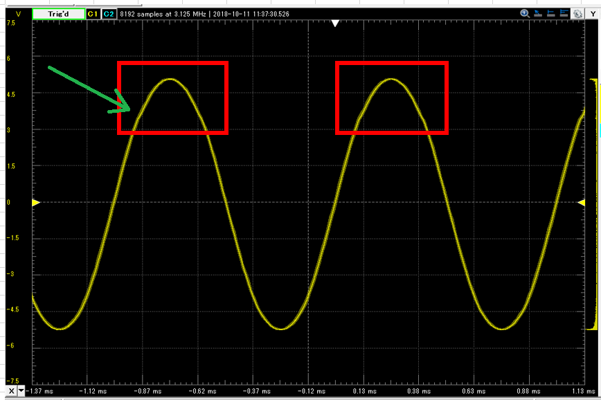
    It seems that this issue is the crossover distortion, so does OPA197 support the true rail to rail input and output such as OPA388 ?

    Best regards,
    Kato

  • Hi Kato,

    yes, I thought exactly the same when I saw theses figures... :-)

    Let's wait what Thomas will say about this...

    Kai
  • Hello Kato-san,

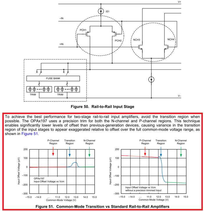
    Figure 51 shows the OPA197 P-ch/N-ch transition region occurs about 2 V below the positive supply rail. When I view the image that Kuramochi-san provided it looks like the distortion is occurring around 1.5 V below the positive rail so it is close. However, Figure 51 shows only about a 50 uV offset change due to input crossover transition. I don't think we would be able to see that small of a change in a DSO image. The left hand voltage scale looks to have 50 mV minimum divisions which are very large compared to 50 uV.

    The other issue is the fact that the distortion goes away when Mic1 (13 pF) is shorted. I can't help but think there is a capacitance non-linearity that occurs with the applied voltage level (voltage coefficient). We have observed voltage level induced distortion in active filters that used a specific capacitor dielectric. At low signal levels the distortion was not present, but as the input voltage to the filter and across the active filter's capacitors increased waveform distortion was observed. Changing the capacitors to the C0G dielectric cleared up the distortion. 

    I would like to give Kuramochi-san an opportunity to investigate and answer my original questions. I am not ruling out input crossover distortion, but I don't want to rule out everything else just yet.

    Thank you much for your valuable inputs.

    Regards, Thomas

    Precision Amplifiers Applications Engineering


  • Hi Thomas-san,

    Thank you for the explanation.

    We can judge whether the root cause is Mic1 capacitor if observing the node voltage between C1 capacitor and GND or between R1 resistor and GND with an oscilloscope.
    I would like to wait for a response from Kuramochi-san.

    Best regards,
    Kato

  • Hi Thomas-san, everyone,

    I answer Thomas-san's questions as below;

    >What kind of capacitor dielectric do the capacitors have (especially Mic1, 13 pF) i.e. X7R, Z5U, C0G, etc.?

    Mic1 is a mica capacitor(called DM5C120J1). It should not have have piezo effect because it is not ceramic capacitors.

    Only Japanese page → www.matsuzakidenki.co.jp/.../

    >Does U1 have power supply bypass capacitors connected from V+ and V- to ground?

    Yes. each rail has 0.1uF capacitor.

    >Would it be possible for you to capture DSO images of the signal at the OPA197 IN+ input and the output signals with, and without, Mic1 (13 pF) shorted?

    Please refer attached file.

    OPA197 waveform.xlsx

    Best Regards,

    Kuramochi

  • Hi Kuramochi-san,

    Thank you for the information.

    Are they data which are obtained using OPA197 with ± 9V ?
    If yes, I believe that this distortion is due to Mic1 capacitor(13pF).
    So, can you capture the node voltage between R1 and GND if removing two OPA197s ?

    Best regards,
    Kato

  • Kuramochi-san,

    Mica capacitors usually have high quality dielectric having a low voltage/coefficient coefficient. Is there any possibility that could substitute the present mica capacitor with a C0G capacitor? The fact that the distortion disappears when the Mic1 capacitor is shorted is indicating something that we just don't understand yet.

    Regards, Thomas
    Precision Amplifiers Applications Engineering
  • Kato-san, Thomas-san,

    Thank you for your advice.
    I think that this mica capacitor is not related to this distortion because this distortion follows V+ rail as I mentioned first post.

    Best Regards,
    Kuramochi
  • Hi Kuramochi-san,

    Is it possible to prove clearly that Mic1 capacitor isn't the root cause ?

    Best regards,
    Kato

  • Hi Kuramochi, hi Thomas, hi Kato,

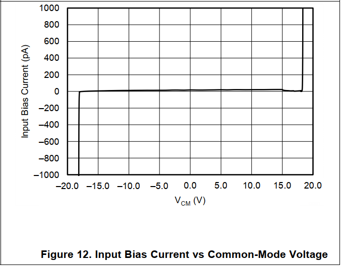
    maybe I'm wrong, but I think it has to do with the nonlinearity of input bias current. We are looking for something that is following the rail and is acting rather sharply, right? The region where the input transits from the N-channel to the P-channel stage is following the rail and causes the input bias current to change sharply, as figure 12 of datasheet shows. Usually, this very little change of input bias current is invisible. But here it becomes visible because the input impedance is extremely high:

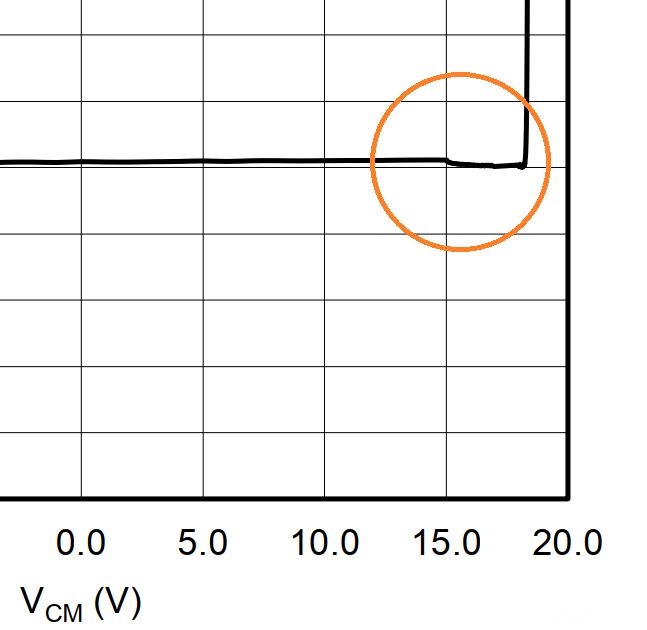
    With zoom:

    When the input voltage rises from 0V on, there's first an input bias current flowing out of the node. It causes a voltage drop across the input impedance which makes the input voltage increase slightly. When the input voltage reaches a point somewhere at about 1.5V...3V below the rail, the input bias current sharply decreases and by this the voltage drop across the input impedance. Because of this the sine gets a break:

    Kai

  • Hello Kai,

    This morning I discussed the various points of the OPA197 input distortion issue with my fellow applications colleague Marek Lis, who has designed a number the TI CMOS precision op amps. Wedo think the distortion coinciding with the N-channel transition region is related to a input bias current as you have described in your response.

    The N-channel devices that are fully operational with a common-mode voltage (Vcm) from about 1.5 V below the positive rail and above are much smaller devices than the P-channel devices active, or partially active, over the remainder of the Vcm range. By virtue of their smaller junction size their input current is less than when the P-channel devices are active. The Fig. 12 graph you provided shows how the input current is reduced in the Vcm region where the N-channel devices are fully active.

    The characteristic that isn't evident in the tables or graph is how the junction capacitances change with Vcm. Indeed the input capacitance of an on CMOS transistor is different than that of an off CMOS transistor. So as Vcm moves from the negative supply rail level, through the entire input range to the positive rail, the input capacitance of the OPA197 changes. This would be especially notable at a Vcm point where the P-channel devices are fully off and the N-channel devices are fully on. The effect of changing capacitance and changing input bias current would be most evident at that point.

    Kuramochi-san's circuit uses an exceptionally high value 30 Gigohm input bias current return resistor. I suspect that the input current change due to the charging/discharging of the junction capacitances at the transition point is resulting in a voltage change at the input. The input circuit consists of an ac voltage divider and shorting Mic1 lowers the source impedance considerably compared to when it isn't shorted. That would affect the charge/discharge characteristics  of the circuit much reducing the minute voltage change at the input transition point.

    Regards, Thomas

    Precision Amplifiers Applications Engineering

  • Hi Thomas-san & Kai-san,

    Thank you for the explanation.

    I understood, so could you please tell me how to improve this issue in detail ?

    Best regards,
    Kato

  • Hi Kato,

    as I said earlier: A remedy could be to increase the supply voltage or to decrease the input voltage and by this keeping the input signal well away from the transition region.

    Kai

  • Hi Kai-san,

    Thank you for your prompt reply.

    I have one more question, so could you please tell me if there is an available operational amplifier instead of OPA197 ?

    Best regards,
    Kato

  • Dear Kato,

    Thomas should answer this question.

    Kai
  • Katso-san,

    The OPA197 input design is a set design and the observed behavior occurs due to the unique set of extremely high source impedance and large signal operation that exercises the full common-mode input range. The OPA197 design is set so we can't look at changing anything there. Here are some thoughts:

    • Kai's suggestions - "A remedy could be to increase the supply voltage or to decrease the input voltage and by this keeping the input signal well away from the transition region." If either of those ideas can be accommodated they should provide a solution.
    • If the input voltage RC divider can be changed to reduce the applied common-mode voltage such that the N-channel transition region is not crossed, the reduction in the input signal level could be compensated for by running the OPA197 in a gain a little higher than +1 V/V. A small increase in gain should have minimal effect on THD.
    • I suspect that the reducing the 30 Gigohm resistor by a factor of 10x (or more) and increasing the input capacitors by 10x (or more) would reduce the offset change effect at the N-Channel transition. The issue then becomes how the microphone response is affected by the change in load impedance.
    • All of TI's high voltage precision op amps use P-channel/N-channel designs to achieve the rail-to-rail input common-mode voltage range so this effect is likely to be observed to some extent with other precision amps applied in an extremely high source impedance application.

    Regards, Thomas

    Precision Amplifiers Applications Engineering

  • Hi Thomas-san,

    Thank you for the information.

    I understood.

    Best regards,
    Kato

  • Team,

    Thank you for your strong support!!!

    Best Regards,

    Kuramochi

  • Kuramochi-san,

    Our pleasure to assist you with your OPA197 inquiry. I think we all learned something new about P-channel/N-channel input behavior when used in a very high source impedance application.

    If you could close this E2E inquiry that would be helpful to us.

    Dewa mata, Thomas

    Precision Amplifiers Applications Engineering