This thread has been locked.

If you have a related question, please click the "Ask a related question" button in the top right corner. The newly created question will be automatically linked to this question.

TPS63700: Power-off with power switching noise

Part Number: TPS63700

Good morning,
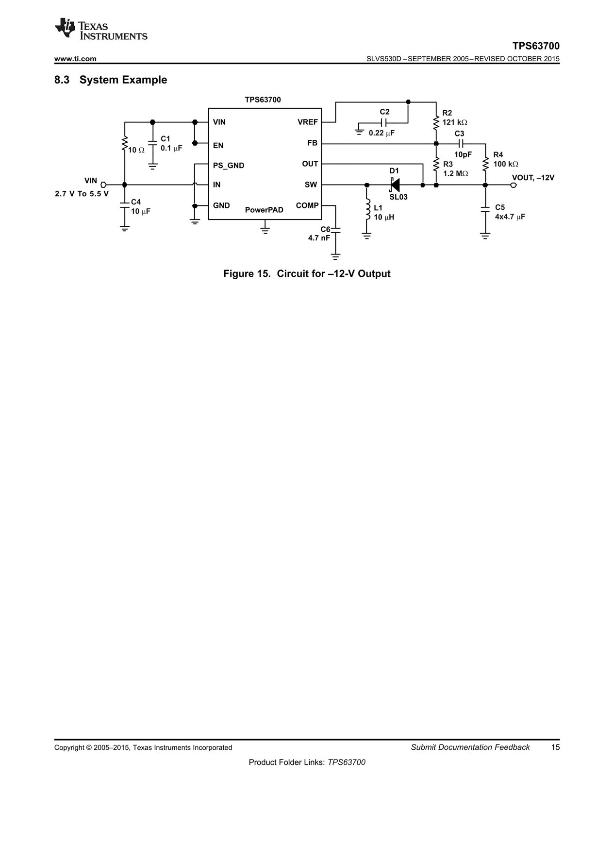
I'm using the component with 5V input and output -12V implemented with the wiring diagram of the attached datasheet. The circuit is part of a board where there are power switches that inhibit the output of the TPS.
To solve the problem, since I could not modify the layout, I reduced the impedance of the external resistor divider connected to the FB pin, with 30K2 between Vref and FB and 300K between FB and Vout. The operation is regular and the stability is good when the load changes, but in this way the current coming out of the Vref pin is about 40µA. I would like to know what is the maximum current that can be supplied by the Vref pin so as not to compromise its operation. Thank you

Greetings

  • I want to apologize for the lack of response on this thread. This was dropped due to a bug in our system.
    Can you confirm you still need the question above addressed?
    Thanks,
    Jim Carrillo
    Manager, Online Support
  • Good morning Jim,

    I need the answer to know if I can implement the change without problems of reliability, thanks.

    Best regards

  • Hello Sandro,
    The Vref of TPS63700 is specified at 10uA.
    This value is also the tested value.

    Since Vref is not tested above 10uA, this should be the maximum that can reliably be sourced.

    40uA is out of device specifications and definitely not recommended.

    Other users who have tried to source more than that have experienced problems.
    Vref output will fall out of tolerance and it does present an IC reliability issue.

    Your description of your "problem" is somewhat vague.
    Can you elaborate?
  • Hello Sandro,
    Is there any more assistance TI may provide you on this topic?
    I look forward to your reply.
  • Hi Ed,
    TPS is sensitive to disturbances from nearby sources. The TPS is the only component on the board that has operating problems, inhibiting its output. If it is not possible to lower the impedance of the divider perhaps I will have to replace the component. I am working to see if it is possible to reduce the present disturbances, I can ultimately feed the divider with a Vref external to the TPS, even if this forces me to modify the PCB.

    Regards

  • Hello Sandro,

    To be honest, I doubt that driving the divider from an external source would reduce the disturbance on the FB node. I think you would increase the problem even more due to additional parasitics on the board.

    Instead you could try to add a very small capacitor in parallel to the resistor between FB and VREF to make the feedback less susceptible to noise. Please use a resistor of at least 120 kohm from FB to VREF. Now start with a 10pF cap in parallel to this resistor to generate a low impedance path for the noise to GND through this and the VREF cap. I cannot guarantee that it works, but it is worth a test.

    Then a change of the layout would be necessary as well, but you keep the VREF current in a save range. Before you change the layout, it is as well important to review it to make sure that you reduce the noise coupling into the FB node is a lot lower. This normally can be achieved by a layout change.

    Best regards,
    Brigitte
  • Hi Brigitte,
    The divider from an external source was however with a reduced impedance, ie 30K from FB to VREF and 300K from Vref to VOUT as I had done at the beginning. As for the capacitor from FB to VREF, I definitely try to insert it and let you know.
    Thank you
  • Hello Brigitte,
    I tested the capacitor in parallel with the 121K resistor between FB and VREF, below the results in the presence of disturbances:

     10pF: not effective
     22pF: the output lowers of 600mV
     47pF: the output lowers of 470mV
     100pF: the output lowers of 380mV
     220pF: the output lowers of 240mV
     330pF: the output lowers of 180mV
     470pF: the output is stable
    If there are no problems I would use the solution with 470pF.
    I await your info, thanks.

    Best regards
    Sandro
  • Hi Sandro,

    I don't think that a 470pF in parallel with R2 is a good idea. There must be a different cause why the switcher is performing improperly. Changing the feedback components is the worst way to "solve" the problem, because you massively impact the stability of switcher by these changes.

    What are the "disturbances from nearby sources" you mentioned above? Why not shielding the switcher from these "disturbances"? That would make a lot more sense than fumbling with the feedback components of switcher.

    Kai

  • Hi Kai,
    they are not irradiated disturbances, here the shielding is not necessary I have already done a lot of tests on this.
    In addition, the app is already in production I can not overturn everything. Welding a capacitor on top of a resistor does not create big problems, I point out that fortunately not on all cards the TPS stops working, they are about 20/30% even if those that work have the output that lowers a lot.
    The component is mounted on a board that generates high voltage with a HV transformer driven by a full bridge resonant circuit by means of a mosfet. The bridge is powered by a PFC which generates a 380Vdc Vbus.

    Sandro
  • Hello Sandro,
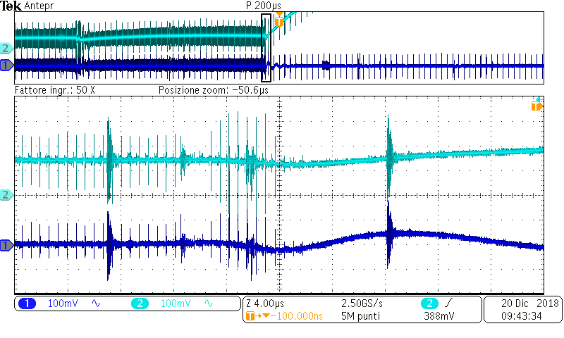
    Can you post some pictures of what the upset looks like?
    Vin Vout Iout during the event.
  • Hi Ed,

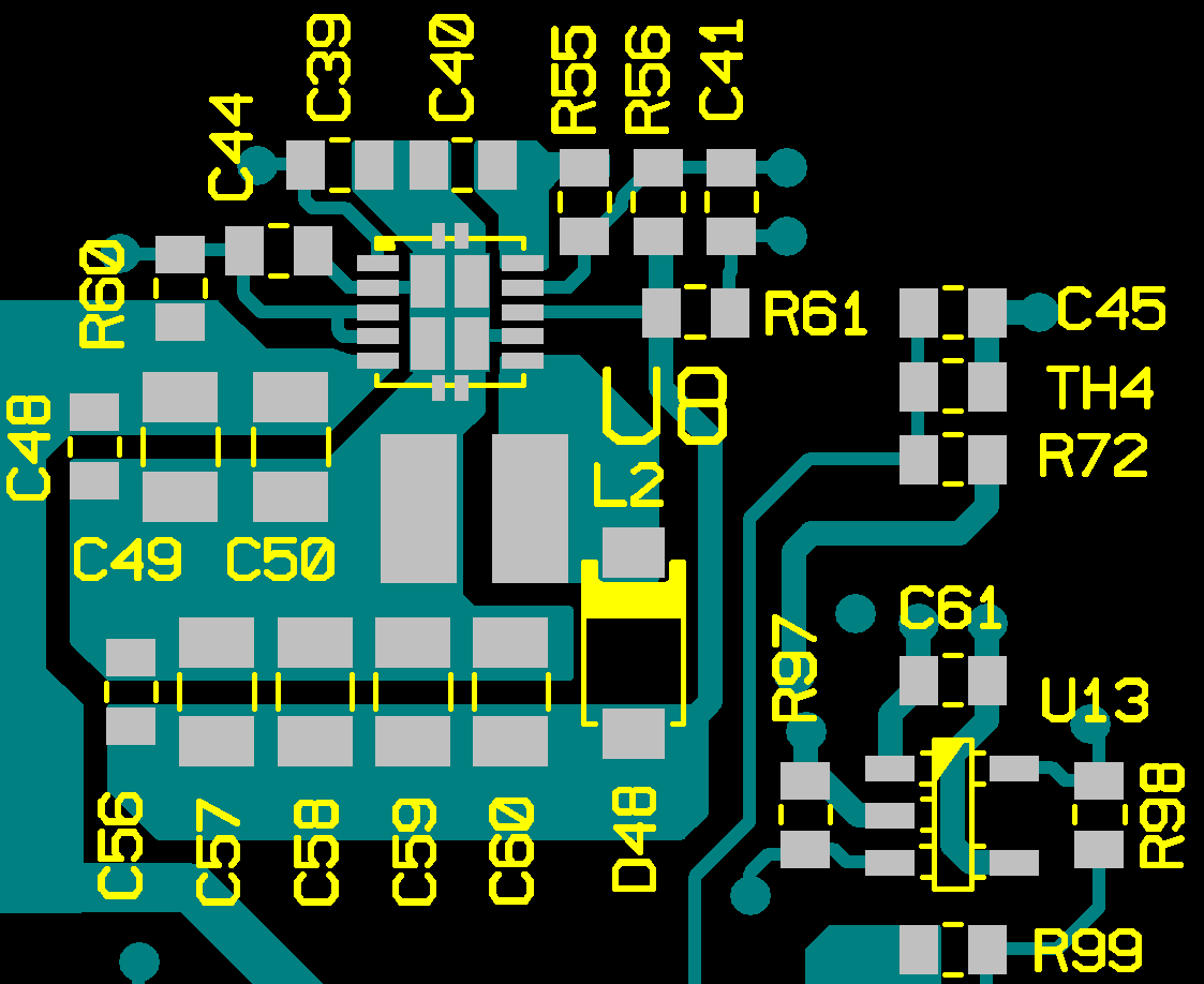
    I send you the acquisition at the time of switching off the TPS in relation to the increase of disturbances, moreover the gerber with the comparison of the components with those of the datasheet.

    Layout Wiring diagram of the datasheet
    C49,C50 = 4,7uF C4
    C48 = 100nF  C4
    R60 = 100 Vin 10Ω
    C44  C1
    C40  C2
    R55  R2
    R56 R3
    C41 C3
    R61 R4
    C39 C6
    L2 L1
    D48 D1
    C57, C58, C59 ,C69 = 4,7uF C5
    C56 = 100nF C5

    TPS63700: Ch1 Vin, Ch2 Vout

  • Hello Sandro,

    The capacitor you need to connect from feedback to GND is big and this will reduce the bandwidth of the converter. I think it is better to check out if we can reduce the disturbance.

    When I checked you layout, I could observe that the feedback is directly connected to the anode of D48. This means that the output capacitors do not really filter the noise on this pin and it will be injected into the FB node. I recommend to try on some boards that show the failure to cut this line and connect via a blue wire to C56. I hope that this reduces the noise injected into the FB node.
     

  • Hi Brigitte,
    I tried to do what you say but it did not work, I think that eventually the solution of the condenser may be the only way to go, accepting a slight lowering of the voltage with a capacitor lower than 470pF.

    Greetings
  • Hi Sandro,

    figure 16 of datasheet shows a layout recommendation with a star-connected GND wiring. Do you see the gap between the input GND and output GND? Figure 18 also shows this star-connected GND wiring. Why haven't you adopted this technique in your layout? The idea of this scheme is to separate the output current spikes from the input wiring and by this to avoid an undesired feedback.

    Brigitte already mentioned that the feedback trace is improperly connected to the output caps.

    Another issue is the switching diode D48. Section 10.1 of datasheet says:

    "The diode need to be connected closest to the SW pin to minimize parasitic inductance."

    And in fact the recommended layout of figure 16 of datasheet has this diode placed directly next to the switcher. But in your layout the diode is far away from the switcher.

    Section 10.1 also says:

    "If the layout is not carefully done, the regulator could show stability problems as well as EMI problems."

    And that's exactly what you observe right now. The TPS63700 is a 1.4MHz switcher which does not forgive the slightest layout mistake.

    With the adding of 470pF cap you will cure a mistake with a second mistake. This will not solve your problem but only furtherly decrease the stability of switcher and degrade the overall performance. It's your decision...

    Kai
  • Hello Sandro,

    The capacitor from FB to GND has to be small enough to not influence the DC value of the converter at all and shall only operate as a high-frequency noise filter. Therefore I recommend a layout change in this case.

    When you mention "it did not work", does this mean it did not change anything or the change was not enough for your system to work properly. The test was not to solve the problem but to check if a positive trend can be observed when you do this change.
    In general a layout issue cannot be solved by changing external components or doing blue wiring.

  • Good morning,
    unfortunately in this case the layout is not my work, I am absolutely convinced that the reason for the problem is the incorrect layout, certainly in the design phase we did not expect such an accentuated criticality, also due to the fact that it is the first time we use the TPS, I will see to carry on the remake of the layout. I conclude with heartfelt thanks to all those who have helped me to understand the problem.

    Sandro

  • Good luck and

    Buon Natale!

    Kai
  • Ciao Kai,
    Buon Natale to you too!

    Sandro
  • Hello Sandro,

    Please ask the person doing the layout to have a look at the layout of the EVM and check the layout rules given in the datasheet. Hopefully this helps.

    I wish you a peaceful time during the Christmas vacation.

    Best regards,
    Brigitte