This thread has been locked.

If you have a related question, please click the "Ask a related question" button in the top right corner. The newly created question will be automatically linked to this question.

THS4303: Two stage of THS4303

Part Number: THS4303

Dear support,

When I put two THS4303 amplifiers in series, I get some oscillation, the first one is around 700 MHz.

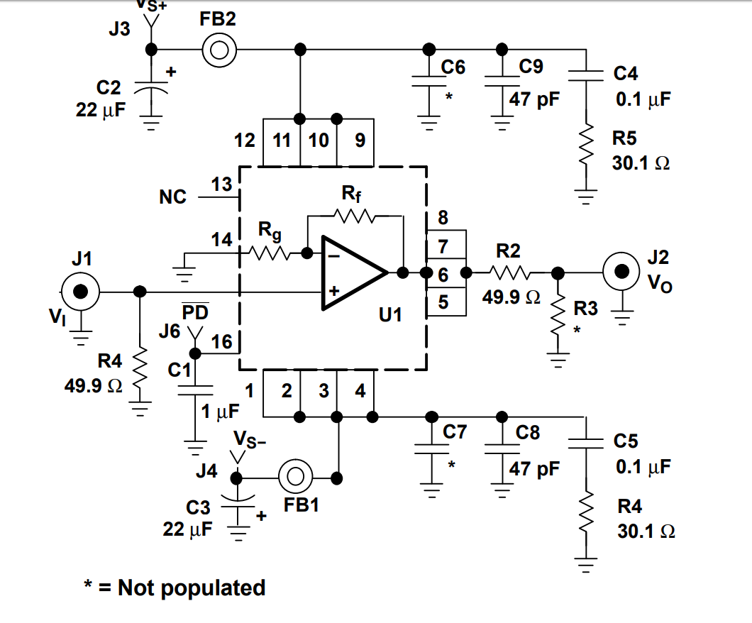
I used the configuration below for each stage.

Can you please show me how to kill these oscillation and which configuration I need to use for each stage? 

Best regards,

Hamza

  • Hi Hamza,

    Apologies for the delayed reply. Are you able to share any of your PCB layout of the circuit? With fixed gain amplifiers, oscillations are most likely due to parasitic issues on the device pins.

    Regards,
  • Hi,

    Thank you for your reply, I'm really in need of help.

    Yes sure you can find below the pcb layout that I used for measurement.

    Best regards,

    Hamza

  • Hi Hamza,

    your layout should look much more like the recommended layout shown at page 21 of datasheet. So, you need much more ground fill in the middle of your board. The THS4303 must be fully embedded in the ground plane of top layer, like shown in datasheet.

    Another issue is your connection between the two THS4303. This connection must be routed as a 50R microstrip line. So, it should be much wider and should also be embedded in the ground plane of top layer. It's not enougn to route a simple copper track. It must be a 50R microstrip line. Have again a look at page 21 of datasheet to see how this is done in the example layout.

    The input and output tracks, these must also be 50R microstrip lines.

    All the components which are connected to the THS4303 must sit much closer to these chips. Have again a look at page 21 of datasheet to see how this is done in the example layout.

    The leads on each side of THS4303 (having the same signal) must be soldered onto one thick copper track, not onto four thin copper tracks. Have again a look at page 21 of datasheet to see how this is done in the example layout.

    Your layout should look like two EVMs placed next to each other with the output of first EVM directly connected to the input of second EVM.

    Why not taking two EVMs for your application?

    Kai
  • Hi Kai,

    In fact, I used the pcb layout that I sent you with one stage EVM and it works fine. But when cascading two of them, either I get oscillations or high current consumption. Can you please clarify why we get this high current consumption? what could be the reason behind this behavior?

    I will of course design new pcb with this new design considerations.

    Do you recommend using the same bias lines or separated ones for the two EVMs? I mean do I need to take voltage to the other EVMs after the 47 pF or before the 22 µF capacitor?

    Best regards,
    Hamza
  • Hi Hamza,

    each amplifier has some stability reserve and can handle some layout mistake. That's why your layout might have worked with only one stage. But at some point the circuit turns unstable. That's when you have cascaded two of them.

    High current consumption often is an indicator for osciilations. These oscillations can usually be seen at the output of OPAmp. But sometimes only the input stage of OPAmp oscillates while the output seems to be stable. In this case the current consumption of OPAmp can heavily rise.

    C2, FB2, C9, C4 and R5 form a PI-filter. A Pi-filter only works properly when the components are sitting very close to each other. Have a look at page 21 of datasheet to see how this is done in the example layout. And each OPAmp needs to have it's own PI-filter, sitting closest to the supply pins.

    Kai