This thread has been locked.

If you have a related question, please click the "Ask a related question" button in the top right corner. The newly created question will be automatically linked to this question.

INA223: 0.1Hz to 10Hz Voltage Noise Measurement

Part Number: INA223
Other Parts Discussed in Thread: OPA827,

Hi Sir


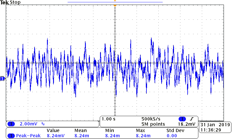
For correlating figure 28 “0.1Hz to 10Hz Voltage Noise”

We builds up active filter as TI verified design mentioned in document #SLAU522

And take OPA827 as DUT, briefly connecting and wiring without shielding can.


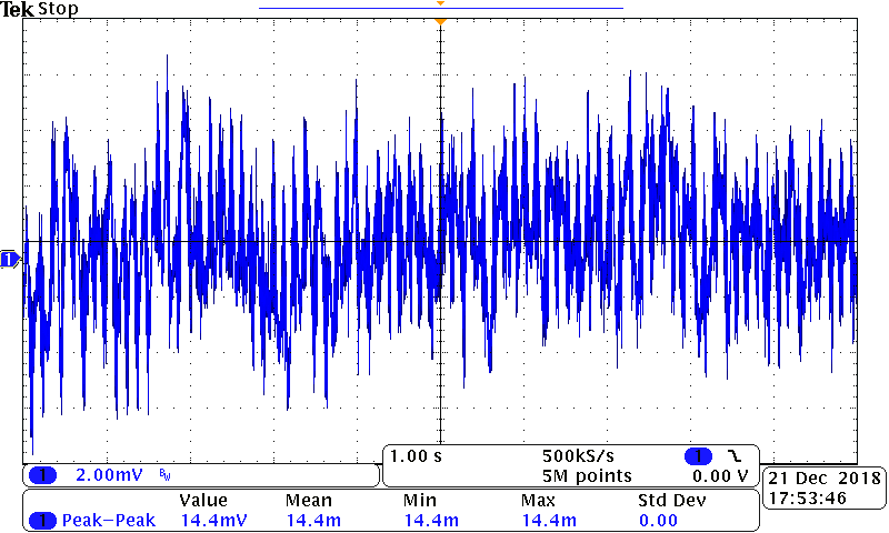
The resulting waveform is approximate and satisfied as the attachment (PK-Pk = 24.2mV) but not INA223 while using as DUT instead


OPA827


According to figure 28 of INA223, the estimation should be


(1) Gain = 20

VOUTPK-PK = 200nV/ Div x 6 Div x 20 (Gain) X 100 (Filter Gain) = 2.4mV


(2) Gain = 300

VOUTPK-PK = 200nV/ Div x 1 Div x 300 (Gain) X 100 (Filter Gain) = 6mV


The resulting is 10 times more than expectation; we have no idea what dominate the measurement, and how to identify


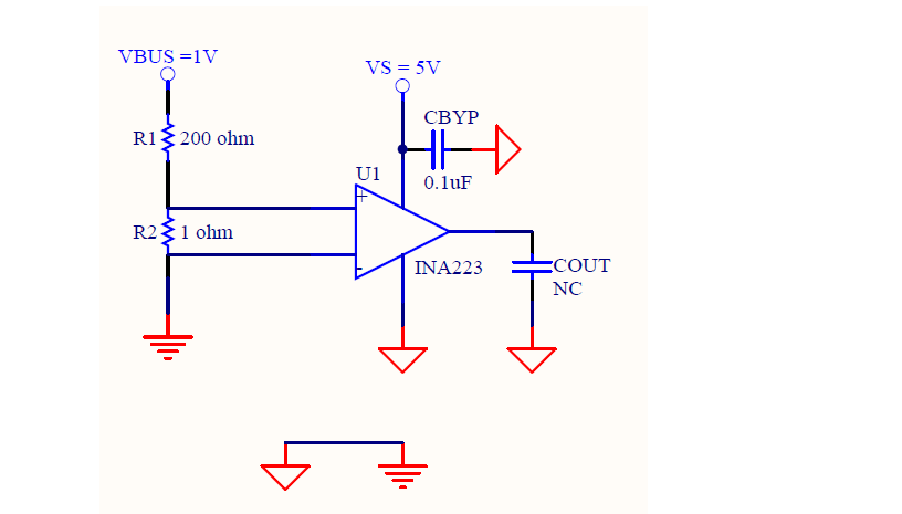
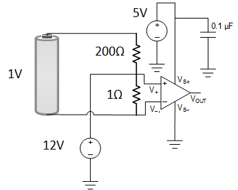
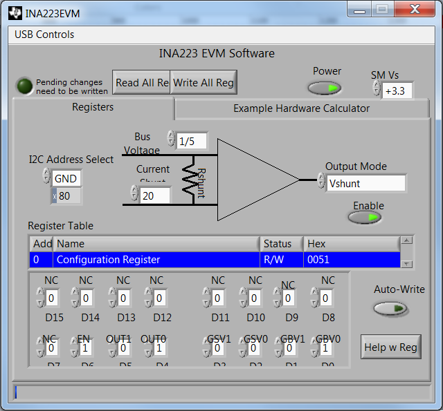
We simply set VCM about 1V and VIN+ - VIN- is about 5mV via voltage divider (200 ohm and 1 ohm), tie VIN – to GND.


Thanks for recommendation and measurement guide!

Regards

Ben


  • Hello Ben,

    Thanks for considering to use Texas Instruments. What are you using to supply the input? If it is an AC to DC converter plus a switch mode power supply source, that can potentially introduce a lot of input noise even with a large cap across the VCC and GND. For the lowest input noise, you should use a battery. One of the best battery sources you could use would be a NiCad battery.
  • Hi Patrick

    Thanks for recommendation!

    Actually the differential voltage developed across is from the dividing of linear power supply or Alkaline battery

    Where

    VS = Linear power supply

    VBUS = Linear power supply or Alkaline battery

    Conventionally the output noise of OPA is measured by shorting the input to GND.

    As understanding, the incorrect input common mode voltage will lead INA incorrect as well

    Since INA is symmetrical and balanced, is it suitable to connect the both inputs to GND?

    Or all I have to do is to find a clear source?

    Is it possible to show how you measure the noise of INA?

    Regards

    Ben

  • Hello Ben,

    Can you set up the INA223 like shown below?

    Also one test you could do is measure the noise of the output for the following configuration.  This will show if these op amps are contributing more noise than expected.

    Lastly, if you apply a 1mV sine-wave at the input here, do you see a 100mV sine-wave output?

    At the moment having some difficulty tracking down the engineer and the test apparatus used for the noise measurements we took.  Will let you know when I am able to track them down. Also I would not connect the inputs of the INA223 to ground for your measurement.

  • Hi Patrick

    Thanks for the reminder and comment!


    The transfer function and noise floor of BPF have been checked.

    The corner frequency and gain are close to your design but I am not sure what the expectation of noise floor is. since there is no mention in this document # SLAU522

    Noise floor of BPF

    INA223 @ Shut voltage mode (Gain =20V/V)

    According to the waveform, the pk-pk is much worse than expectation

    Please refer to the set-up picture, is there anything required to have an improvement? Maybe I should not take something as granted!


    Appreciate for paying much attention and effort on this case


    Regards

    Ben


  • Hello Ben,
    When you say the gain is close, does that mean when you passed a 1mV signal at 1Hz and saw a 100mV output? If it was greater than 100mV, how big was it? I noticed that your fabricated board is a little different than what is shown in SLAU522. Can you give me a list of the board modifications you made? As for your setup, could you this time include the INA223 and ground the inputs. Also can you set the output mode to shunt voltage measurement in the configuration register if you have not already done so previously?
  • Board Modification for INA223 20190110.pptxBoard Modification for INA223 20190110.pptxHi Patrick

    Thanks for reply and sorry for not describing clearly!

    Patrick:

    When you say the gain is close, does that mean when you passed a 1mV signal at 1Hz and saw a 100mV output? If it was greater than 100mV, how big was it?

    Ben:

    Yes! Where the close gain and corner frequency I mentioned is the active BPF (I am trying to matching the components as the design recommended as possible)

    Patrick:

    I noticed that your fabricated board is a little different than what is shown in SLAU522. Can you give me a list of the board modifications you made?

    Ben:

    Please find the attached ppt for more details, Basically, the difference is for INA223 only and leave others unchanged.

    Patrick:

    As for your setup, could you this time include the INA223 and ground the inputs.

    Ben:

    Does it mean tie both input to GND directly as conventional noise measurement of OPA? As memory, you would not connect the input to GND for this measurement, what is the intention for grounding the input to GND this time?

    Patrick:

    Also can you set the output mode to shunt voltage measurement in the configuration register if you have not already done so previously?

    Ben:

    Also I am always configuring the measurement to shut voltage mode, thanks for reminder!

    Patrick:

    At the moment having some difficulty tracking down the engineer and the test apparatus used for the noise measurements we took.  Will let you know when I am able to track them down

    Ben:

    Is it possible to track them down?

    Ben:

    I am planning to make a board revision, please find the same ppt for reference as well.

    Any recommendations and ideas are welcome

    Regards

    Ben

  • Hello Ben,

    The intent of having both inputs tied to ground was to remove any noise that comes from the common mode supply. In hindsight, this part is a unidirectional part and it would be better to have a IN- tied to ground with the voltage divider output from the battery tied to the IN+.

    Unfortunately I was not able to track down the engineer responsible for those measurements. Consequently, I am building up my own noise filter board to collect my own noise measurements. Once I have collected some measurements, I will update you on any tips or recommendations. This may take a few days. Sorry to keep you waiting so much.
  • Hi Patrick

    Appreciate for continuing paying much attention on this measurement!

    This item is the most critical in the precision measurement!

    Much more time consumption is reasonable but it is worthy.

    I am also studying anything possible to make this measurement better!

    To make sure what I understand clearly and avoid any misleading, I may draw a simple schematic for discussing!

    (1) Stimulus from battery

    (2) Tie both inputs to GND

    Does it also require? (Too much closer to GND)

    I am going to follow your recommendation once the revised board is available.

    Looking forward to your own measurement and another application report publication as SLAU522, that someone can easily Google it and get satisfied guide to the beginner as me

    Regards

    Ben

  • Hi Ben,

    I hope you shield the whole circuit? Put the OPAmp circuit into a shield and experiment with the best GND connection for this shield. Properly shielding can dramatically improve the noise performance!

    Kai
  • Hi Kai


    Thanks for recommendation!

    I made a brief ptt file to show how the measurement is taking

    Since the revised board is not ready, I using the previous one still


    INA223 Set up for noise measurement.pptx


    Have you ever evaluated the shielding effectiveness of mental box?

    I put a mobile phone inside the box and make a 3G/4G phone call,

    but the ringtone is still perceived.

    As you mentioned, properly shielding can dramatically improve the noise performance, I have no idea how to define the “properly”


    Regards

    Ben


  • Hi Ben,

    I would connect the enclosure to the signal ground near the DUT.

    To shield cell phone radiation the shield must not have even the smallest gap or break!

    One way to improve the shielding effectiveness is to use several shields following the onion-shell principle. So, you could have your big metal enclosure AND an additional shield close to the DUT itself. The inner shield should be connected to signal ground as close as possible to the DUT.

    A good noise measurement can be really tricky...

    Kai
  • Hi Kai


    Thanks for recommendation!

    Would you make sure the shielding effective before making noise measurement?
    (I simply check the connection of cellular phone, is it necessary to confirm the wireless connection failed? how about yours?)

    Regards
    Ben
  • Hi Ben,

    the best indication that the shield is working as intended is when the noise level goes down. :-)

    During the noise measurement I would just forbid the use of any cellphones, ipads, etc. near the setup. Also, turn-off any device which is not used for the measurement. Turn-off all fluorescent lamps. These are very noisy! Do also pull out all irrelevant mains plugs. Keep all mains transformers well away from the setup.

    Kai
  • Hi Kai


    Thanks for recommendation!
    Noise is everywhere; Other than Lab, I should move all the setup to another quite room (we have no dedicated chamber, meeting room may be suitable) and keep away from any electronic devices


    Due to difficulty of the correlation to the result of datasheet
    I am very curious that whether it is possible to have an estimation for the contribution of INA223 itself?

    Since the output show the overall noise distribution? INA223 and others

    RMS (Overall) = RMS (INA223) and RMS (Others)

    If the noise distribution of others is realized,

    It may be a good alternative


    Regards
    Ben
  • ello Ben,

    Sorry about not getting back to you sooner.  I tried duplicating a setup similar to yours and I also got measurements that were larger than what is shown in Figure 28 of the datasheet.   Upon investigating this, I think there may be a scaling issue with that figure as there is a discrepancy between this figure and the collected data.   Despite this, we do have a 0.1 to 10 Hz noise specification in electrical characteristics section of the datasheet called voltage noise density.  Based of this specification we can calculate the typical peak to peak noise we would expect to measure.  To calculate this we take the number provided in the specification and multiply by the square root of the upper bound of the bandwidth and we also multiple this by 6 to convert from RMS to peak-to-peak. This gives us (235nV/sqrt(Hz))*sqrt(10Hz)*6=4.46uV.  This actually correlates well with some measurements I was able to make.  

    For my setup, I added an additional gain stage in front to ensure, I would not have any issues with running into the noise floor of the SLAU522 board.  The reason I did this is that the SLAU522 board is designed for a high gain (1000V/V) dut.  The added gain stage utilized another opa827 with a 50V/V gain. From cascading my INA223 in series with the added gain stage and the original gain stages, I got an output with 450mV peak to peak.  If I divide out the gain I get 0.45/100/50/20= 4.5uV peak to peak referred to the input noise.

    For my setup I used a copper clad box to help shield out external noise sources. I also used a linear power supply to power the OPA827 gain stages as opposed to a switch mode power supply that couples more noise into the supplies.  From this linear supply I used the shortest connector leads I could to reduce how much noise they might pick up.  As I used solder with water soluble flux, I cleaned the board with a ultrasonic cleaner to reduce the impact of flux creating additional parasitic paths.   For my setup, I actually ended up using separate pcbs for the INA223 and the filter gain stages.  The INA223 board was our standard EVM that can be powered and programmed through a SM-USB-DIG connected to a laptop.  As the SM-USB-DIG that converts USB to I2C potentially could contribute noise, I dangled this part outside of the copper clad box.   On the scope I used a direct 1x probe DC coupled to ensure that the scope did not filter out any of the desired lower frequency content.  My measurements, board, and setup can be observed below.

  • Hi Patrick

    Thanks for much effort on reproducing the waveform!

    It is very detailed and clear description what and why you are doing

    Voltage noise density of INA223, I consider it is a typo and neglect at the first sight, since the representation is different between INA223 and OPA827, one show density the other is peak to peak

    I am referring the result of waveform recently collected to the input

    8.24mV / 100 / 20 = 4.12uV

    According to your calculation, the input voltage noise is 4.46uV typically

    It is highly correlated

    Could you please help update the noise waveform to the datasheet officially?

    Regards

    Ben

  • Hello Ben,

    I cannot simply swap the plot out in our datasheet due to the internal approval process we have in place. To push the change forward, will require further investigation. This investigation would start with discovering the source of discrepancy between that figure and some measurement data I was able to find. As this data was collected 7 years ago, finding the source of error will be difficult.

    In the meantime I encourage you to work with the specifications provided in our electrical characteristics section. The values for noise density from the table resulted in 0.1 to 10 Hz calculated noise which was in agreement with what I was able to measure in the lab. If you measure noise significantly lower than this there is very likely an error in the setup or calculations.

    As we have provided the methods for improving your noise measurements and we now have figured out how to correlate my measurements and your measurements with the datasheet electrical characteristics table, I believe have serviced your initial issue and will therefore close this thread. However, once we have any developments for changing the plot in the INA223, I will be sure to let you know.