This thread has been locked.

If you have a related question, please click the "Ask a related question" button in the top right corner. The newly created question will be automatically linked to this question.

LM7322: P/N: LM7322MAX/NOPB conspicuous resistance values measured on some parts between pin1-4

Part Number: LM7322

**** SO# 446657 ****

Hello,

our customer mentioned tat they have 8pcs failed of 2500 purchased during the ICT test.
Between pin 1 and pin 4, a resistance of approx. 30 - 200kΩ is measured. 

The "good" components show a resistance of >= 10MΩ. These components were soldered.
- For a piece that has not yet been soldered, the resistance between pin 7 and pin 4 is about 100kΩ. The resistance between pin 1 and pin 4 is >= 10MΩ.

But there are no failures during functional tests.

The question is,
- whether the conspicuous resistance values ​of approx. 30 - 200kΩ for the affected components are ok?
- in the long term it can be assumed that this can lead to field failures...?

Can you please advise?

Thank you.

  • Hi Adnan,

    pin 1, pin 4, pin 7 of what?

    You should show us a schematic...

    Kai
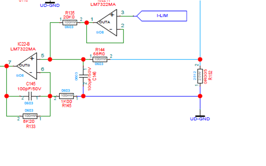
  • My apologies Kai, I forgot to add the schematic of the part showing the pinout:

  • Hi Adnan,

    I'm not clear why someone would want to measure the resistance between pin 1 and pin 4 of LM7322 or between pin 7 and pin 4. The resistance between these pins isn't specified in the datasheet at all. And I don't know what insight this should give to find out whether the LM7322 is working properly in the product later or not.

    Sorry, but this really sounds weird to me.

    Kai
  • Adnan,

    Device pins have non linear characteristics. Too much voltage could actually power on the part.
    What is the voltage (and current) for these ICT resistance tests?
  • Adnan,

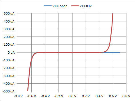
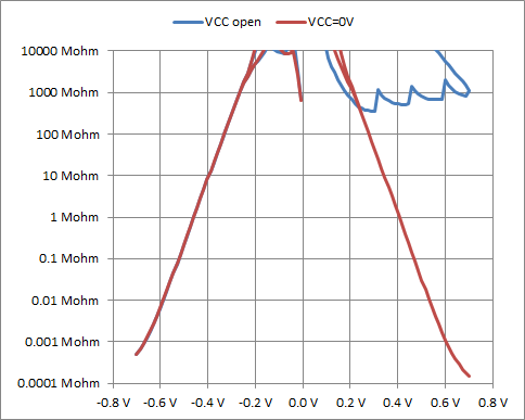
    Here is data I just recorded for pin 1 to pin 4 with pin 8 open or 0V.

    Pin 1 Current vs. Voltage

    Pin 1 Effective resistance V/I vs. Voltage

  • Hi Ron,

    The voltage for the ICT test is 0.3V.


    The resistor R135 (20k) should be measured. However, the "resistance" from the position IC22 Pin 1 to Pin 4 is apparently also measured, because the resistors R144 and R152 are very low to ground.
    Require confirmation that the internal resistance of the operational amplifier can be undefined.

    Best regards Gerhard Nebel

  • Hi Ronald,

    The voltage for the resistance measurement is 0.3V.
    The resistor R135 (20k ohms) should be measured.
    The resistors R144 and R152 against ground, are low impedance and the resistance of the operational amplifier position IC22 pin 1 and pin 4 (about 30 - 100k ohms), so it probably comes to this "incorrect measurement".
    Require confirmation that the output resistance from the operational amplifier can assume an undefined state.

    Best regards Gerhard Nebel

  • Gerhard,

    The picture did not attach properly. What was the file type? Did you use this feature?

  • Hi Ron

    Insert File *.png.

    I hope, now is right.

    Best regards Nebel Gerhard

  • Hi Gerhard,

    I really don't understand what the issue is. If you want to measure R135, why don't you measure between pin 1 of OPAmp and GND? Why do you measure between pin 1 and pin 4 instead? By doing this you will drive current through dozens of leakage paths, like parasitic pn-junctions of OPAmps and decoupling capacitors. By this you will never get true results, unless all involved caps are fully charged and don't show any relevant DC leakage current under bias voltage like electrolytic caps are well known for.

    With the todays high reliable assembling and soldering this insane "in circuit testing" shouldn't be needed any longer. This made sense at a time when the automatic soldering produced lots of errors. But today? We had so many trouble with the "in circuit testing" that we completely stopped it some years ago.

    Kai
  • Adnan,

    I can see the schematic picture now. The typical "resistance" at 0.3V per my chart is about 30M ohms, therefore the measurement in circuit should be 20.05k ohms.  

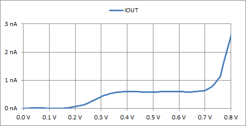
    However, the output transistor is large and has high gain. With power off there is no active turn off for this transistor. Therefore there is some normal current flow. My sample was less than 1nA.    

    For your 30k measurement, was that also at 0.3V? If so then current was 10uA which is quite a bit higher.

    Can you run a simple test on your suspect units? With pin 4 ground, apply [0.1V, 0.3V, 0.5V, 0.7V] to the suspect output pin and measure the current values.

    If the data has the same shape as my chart, then the current is normal transistor current.