This thread has been locked.

If you have a related question, please click the "Ask a related question" button in the top right corner. The newly created question will be automatically linked to this question.

LM124: LM124

Part Number: LM124

Hello,

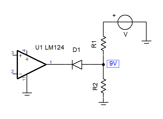
I have question on the LM124. If the VCC 12V supply voltage is open, and the output of Op-Amp connected to a diode (cathode side). On the other side of the diode we have about 9V (through a voltage divider network) . How do I determine how much current sourcing and the voltage at the Op-Amp output pin ?

Best Regards,

Jason

  • Jason,

    Does this match your description?

    We know that Id + IR1 + IR2 = 0; so Id + (9-V)/R1 + 9/R2 = 0

    Solve for Id.

    If you don't have these number because the circuit is not yet built. Then it is more complicated. If output is greater than VCC then current will flow from output to VCC bus which will try to raise VCC voltage. This current flow must be limited to a low value to prevent damage to the LM124. I see that open load voltage is 9V , but what is the thevenin resistance for the voltage divider. In the drawing it would be (R1*R2)/(R1+R2)

  • Hi Ron,

    Thank you very much for quick response. Yes this circuit match with description.  The circuit is built. R1=6.49k and R2= 24.9K, Vcc is about 12V. About 9.5V and 0.4mA flows into D1.

    The 9.5V point is also connected to a FET in a linear regulator circuit. My spice model shows around 3.5V at U1-1 and 1.5mA flow back into the IC (I used Simetrix SPice model with LM124/NS model). I guess there

    is some internal impedance source and current source which will keep this U1-1 low ? If this is not true, could it expose to 9.5V-0.7V = 8.8V and overstressed the IC ?

    Jason

  • Hi Ron,

    Would that possible that I could get the internal circuitry of LM124 ? We are using TI LM124 in  most of our SMPS units.

    Best Regards,

    Jason

  • Jason,

    There is a good schematic on page 10 of the data sheet. However the parasitic diode from the resistor on output pin to VCC is not obvious. The resistor is P doped (think of an anode) and it lives in an N doped area (think of a cathode).  The N doping has to normally be higher voltage than the resistor on the output so it is connected to most positive pin, VCC. This parasitic diode is not made to support current flow so keeping the current flow below 1mA is advisable. Basically the lower the better.

    Be sure to read the new application note for LM124 and its family.

    http://www.ti.com/lit/pdf/sloa277

    On the next revision, I will add this output greater than VCC effect.

  • Thank you for pointing me to the application note
  • Hi Ron,

    Internal of the LM124, there is a Capacitor in the amplifier stage. Could you give me the value of that capcitor

    Thanks

    Jason

  • Jason,

    I'll start by giving you a clue. The current source in data sheet schematic is 6uA and that is the maximum input for cap. The typical slew rate is 0.5V/us when that 6uA gets to the cap. The math formula of interest is Q = i*t = C * v , solve for C.
  • Ron,

    I figure it out by looking at the slew rate of the output voltage and compare with datasheet. I used around 5pF. Based on your equation C = 6uA*8us/12V = 4pF. I put together a Simetrix SPice model and testing it now. Thanks for your help