This thread has been locked.

If you have a related question, please click the "Ask a related question" button in the top right corner. The newly created question will be automatically linked to this question.

THS4140: Gain accuracy

Part Number: THS4140
Other Parts Discussed in Thread: TINA-TI

Hi,

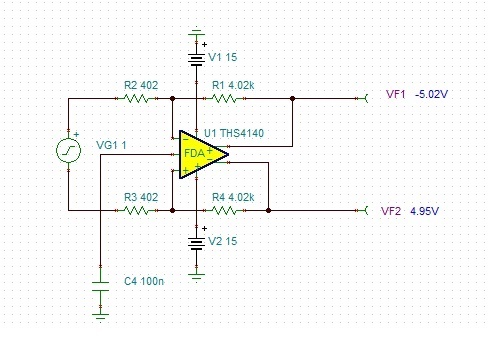
While simulating with TINA circuit with THS4140 for gain = 10, we see that result is not as expected and furthermore, the values of the positive and negative terminals not symmetric.

Rf and Rg are as recommended by datasheet.

As shown in diagram, for the 1V input, the gain is 9.97 instead of 10, and output differential terminals are 50 and 20 mV off (and not symmetrical).

Assumption was that we should be able to see gain = 10, as per recommendations, and symmetrical differential output, in the simulation.

Is the problem in the simulation environment or does it reflect "accurate" device behavior? (can we rely on simulation results in this case?)

Thanks,

Arie

  • Hi Arie,

    this is the result of input bias currents, input offset current and input offset voltages of THS4140. Have a look into the electrical characteristics of datasheet.

    Kai
  • Hi Kai,

    Thanks for prompt reply :)
    In another thread (THS4140: differential input) it was discussed that not all models simulate typical parameters, and specifically it addressed the input offset voltage - since forcing amplifier input to GND, the output in simulation was '0' microV and NOT reflecting datasheet parameter;
    This is exactly the reason of my question, related to this specific device and model, in order to learn from community experience and knowledge what to expect from those simulation results.

    Thanks a lot,
    Arie
  • Hello Arie,

    In the previous E2E post found here: e2e.ti.com/.../768383

    You were not measuring between the inputs of the amplifier but rather between two nodes directly connected to GND. This will reflect 0V in any case. The voltage meter should be connected between the inverting and non-inverting pins of the amplifier to reflect non-ideal effects of the model.

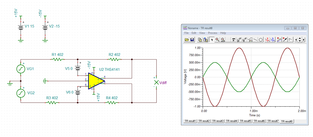
    Also what voltages are you trying to input into the device using VG? Are you trying to input a differential signal of 1V (+500mV and -500mV) or are you trying to provide a DC signal of 1V for both inputs (differential signal of 0V)? The way you provide an input in your schematic does not reflect either case. Putting a voltage source between both nodes only guarantees a differential voltage of 1V but does not guarantee a specific value for either node.

    Best,
    Hasan Babiker
  • Hi,

    In our circuit, there is differential signal feeding the amplifier; this signal range between -1V and +1V, so after the amplifying stage with gain=10 we get output signal between  -10V and +10V.

    My question here was regarding the expected amplified result in simulation, for +1V at amplifier input, because the result we get in the simulation is different than expected ==> should be +10V, 5V on each terminal and we get 9.97V, and the non-symmetric values for positive and negative signals.

    I understand from your comments that you recommend to feed the amplifier input with DC for each positive and negative terminal, as shown in the below

    Is this what you meant?

    If yes, note the result has remained unchanged (still 9.97V and the unsymmetrical values).

    Also, regarding your comment about feeding the differential source to the amplifier, it results in the value mentioned before, so the circuit seems to amplify the input signal, but not accurately ?

    Thanks,

    Arie

    , so this raises another question - 

    So you suggest that in the simulation circuit, I feed the amplifier input with diffe

  • In addition, in reference to the other E2E post ( e2e.ti.com/.../768383) please note that in that post I referred to measurements on the actual board, and probed at the input to amplifier (showing the 4mV value) which would reflect the Vso (input offset voltage), yet doing the same on the simulation didn't show the Vso according to datasheet...

    Thanks,
    Arie
  • Hi Arie,

    now I see your point. Yes, you are right, input bias currents, input offset current and input offset voltages should only shift the signal. But you obeserve a deviation of gain, right? I guess this is an issue of the model.

    Kai
  • Hi,

    Yes, the gain is here the issue and I wanted to know if I can trust the model and simulation to reflect the parameters (I would hope it does) in which case the gain deviation is indeed reflecting the device. On the other hand, if the simulation with the device model doesn't reflect accurately the datasheet, then the interpretation of the gain deviation is different.

    For example if anybody can tell that this simulation and specific model were used and seen to reflect accurately the datasheet, that would help a lot.

    Thanks,
    Arie
  • Hi Arie,

    I would try to contact Ian Williams. He is a TINA-TI and SPice simulation guy, if I'm not wrong.

    Kai
  • Hello Arie,

    There are a few factors that play into the error on the output. The input bias currents should only affect the common mode output of the device Vocm, and there is usually some type of offset on the Vocm pin that will contribute to the 33mV shift. You will also see that there is a slight difference between the two bias currents in the model which will contribute to Vdiff. Your concern of the gain, however, or the change of Vdiff is mostly caused by the differential offset voltage which should be somewhere between 1 to 7mV (from the datasheet) that will be gained by a noise gain of 11 V/V. Taking these factors into account, it is indeed possible to obtain this shift in gain in a real world application, especially with resistor tolerances coming into play.

    Best,

    Hasan Babiker

    Arie.TSC

  • Hi,

    Thanks for all the replies.

    A few notes regarding Hasan's comments - due to same concern with offset impact, I checked in simulation with input of 0.5V instead of 1V at amplifier input, and the value received at the output was 4.98V,

    so 20mV off instead of 30mV.

    I believe that if offset would have been the main cause, I would expect 4.97V (assuming linear behavior)? Do you agree?

    Another thing is the output load - please note that in our simulation we used a high value for the load; we can see that for a load < 1Kohm, there is close dependency between output value and load.

    I assume (and I will also check) that if R5 + R6 in your circuit would be > 1K, the output value would be closer to the 9.97V (and respectively pos and neg terminals values) ?!

    Additional note - well understood and agreed about real life resistor tolerances. In our actual board, we used 0.1% for both Rf, Rg and we measure (with high accuracy DVM) 4.018 Kohm and 401.8 ohm respectively, which is one of the reasons I had to pursue this simulation process, to clarify why the gain seen at the output is off.

    Still, in the specific simulation, the resistor values do not affect the gain deviation, so if I understand correctly, I can trust the simulation results showing the deviation, as reflecting the amplifier parameters?

    Thanks,

    Arie 

  • Hi Hasan,

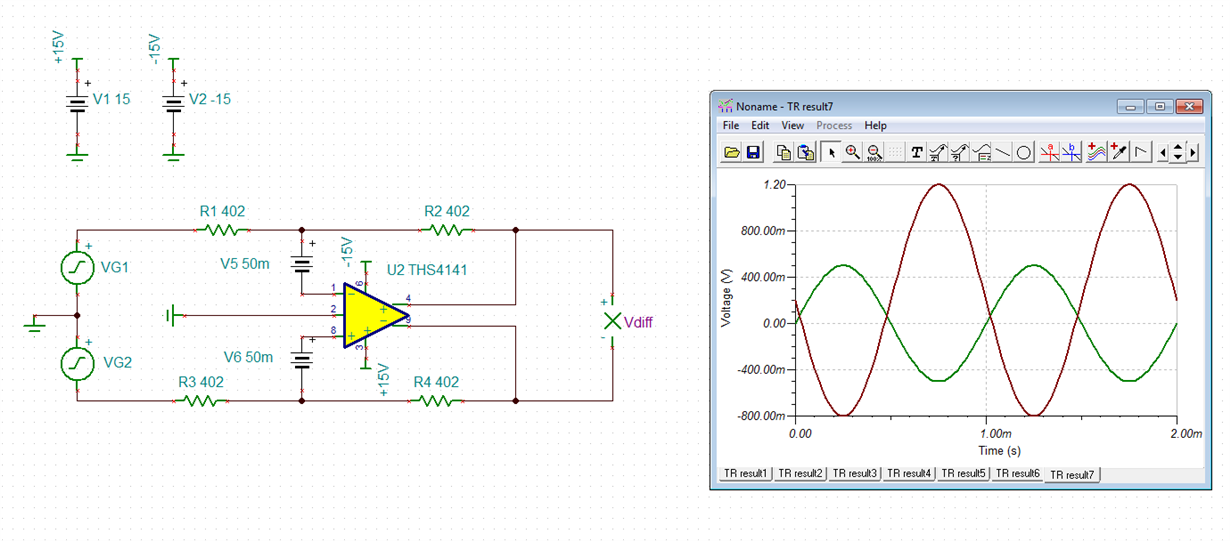
    if it actually was the result of differential input offset voltage, I would expect an output offset voltage shift, like shown in this example. But the output signal amplitude would stay unchanged:

    Arie1.TSC

    This is in contradiction to the result of Arie's simulation, which does not show an output offset voltage shift but a change of gain.

    Kai

  • Hello,

    In regards to your comment Kai, the datasheet specifies two input offset voltage parameters. What I was referring to earlier was the differential offset between both inputs of the amplifier, or in the case of your simulation, a source of 51mV on one side and 49mV on the other to give an input offset voltage of 2mV.

    On your comment Arie, I agree that the gain error should not be increasing along with your input. As this is an older model, I would use it as a general reference but would not expect it to perfectly capture the function of the device.

    Best,
    Hasan Babiker
  • Hi,

    Thank you both.
    So if I understand correctly,the recommendation is not to rely on the simulation results for this case (the gain deviation)?!

    In the real board, I get gain of 9.915 instead of 10 (for values between 0.9913 and 0.995 V at amplifier input, for 5 identical boards).
    Since Rf and Rg used have 0.1% tolerance (verified by measuring resistors with high accuracy DVM - 401.8 ohm and 4018.3 ohm) conclusion was that it must be the device tolerances/parameters, which I tried to analyze using the simulation.
    Thing is that the gain drops to 9.88 (for values between 0.4958 and 4.997 V at amplifier input, for 4 of the same boards mentioned, while the 5th showed 9.93 gain for same value range).
    This tells me it's not offset related, but also not fixed ?!

    What would explain this behavior and what debug steps could help?

    Thanks again,
    Arie
  • Hey Arie,

    Just to clarify, the gain increases to 9.915V/V at the input range of 0.9913V to 0.995V and at inputs above or below this the gain is at a constant 9.88 V/V?

    Best,
    Hasan Babiker
  • Hi,

    The amplifier input is is between -1 to +1V max.
    For input values close to 1V (or -1V) we get 9.91 gain.
    For input values half than that, 0.5V (or -0.5V) we get 9.88 gain.
    As example, for 0.995V at amplifer input, we get 9.868V at the output ( so gain is 9.91)
    And for 0.495V at amplifier input, we get 4.9V at the output ( so gain is 9.88)
    Hope that helps clarify.

    Thanks,
    Arie
  • Hello Arie,

    It makes sense that the gain would improve with respect to your input, since the offset voltage will contribute less to your total output. On the other hand, you mention that the offset is not fixed due to a fifth board giving dissimilar values as the first four. It is worth noting the possible range of the input offset voltage in the datasheet so there can be a variance in gains between boards. It is strange, however, that this specific board improves in gain when decreasing your input.

    Also to your previous question, yes I would recommend not relying on the model for this particular case.

    Best,
    Hasan Babiker
  • Hi Arie,

    I am from an era when we had no Spice models or couldn't afford the Spice simulation software. Later, we found out that the Spice models had so many restrictions that they really weren't helpful at that time.

    From this point of view I would never expect that a Spice model is telling the whole truth. Running a Spice simulation is one mosaic piece of many others during the development. But the Spice model is not the Holy Grail...

    Consider the Spice model as what it is: A nice tool. No more and no less. To be honest, I think, it's much more important to develop the special knowledge and skills to carry out serious measurements during the development phase instead of trusting a simulation too much.

    It's highly welcomed that TI has begun to improve all their Spice models. But this is a long and stony way...

    Kai

  • Hi,

    Thanks for all your feedback, I appreciate it.

    Kai - I couldn't agree more about your comments - indeed no intention to follow blindly any type of simulation and as you mentioned, just "one mosaic piece" more. Still, I hoped to be able to make some use of that as related to the basic functionality - amplification.

    Hasan - I still have the impression that offset, while contributing to, is not the main factor in our gain deviation, and will continue to experiment.

    Thanks,
    Aie