This thread has been locked.

If you have a related question, please click the "Ask a related question" button in the top right corner. The newly created question will be automatically linked to this question.

LMH6552SDEVAL: Issues with differential amplifier

Part Number: LMH6552SDEVAL

Hi everyone,

I am making some tests with LMH6552DEVAL but my outcome is not the expected one. My input is a LVDS signal which has an amplitude of 400mV. At the output, I am looking for a voltage between 0 and -0.5V for the positive cycle and the negative cycle being beyond -3.3V (that's why I have designed for Vcm=-3.5V, to centred the output signal around -1.7V).  I have simulated on TINA my configuration:

I have designed for a gain of 16, having R3=R4=480 ohms and R1=R2=30 ohms. R5=R6=50 ohms are used to adapt the input differential LVDS signal. R10=R11=50 ohm are adapting the output oscilloscope probes (Rosc1 and Rosc2), creating a voltage divider at the output (that's why I have designed for 16 gain instead of 8). Everything looks marvellous in TINA:

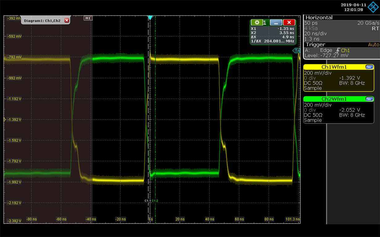
Unfortunately, when I go to the lab and making some tests I have found a non-expected behaviour. My output signals do not oscillate in the range we are looking for but, furthermore, something is wrong with the input V-. Taking a probe with another oscilloscope to measure the input V- I have realised that is being attenuated at the moment that is connected to the amplifier.  The input signal V+ works perfectly but the output signal have the same amplification for both inputs, which does not make so much sense. The only difference between output signals is the offset as can be seen in the figure from the oscilloscope.

At this point I am wondering what can be wrong with the input channel V- and if this could be the reason of the bad behaviour in the output signal. 

Thanks in advance,

Pablo.

  • Hi Pablo,

    Can you upload this TINA file you have created?

    Thanks!
    -Karan
  • Hi Pablo,

    Can I know more information about your application? What is your input source? What gain do you need? If you need a gain of 8 then we can design for that with a center at -1.7V that you need.

    Thanks!
    -Karan
  • Hi Karan,

    The input will be a LVDS input (400 mV amplitude). At the output I want to distinguish a logic 0 between 0 and -0,5V and a logic 1 beyond -3.3V. The next stage will be in high impedance but really close to the operational amplifier, even though I'm adding a 50 Ohm (R10=R11) termination (now the oscilloscope's 50 Ohm). So, I need an amplification of 8, to have a swing between [0,-0.5]V and [<-3,3]V but with the voltage divider created by the oscilloscope input impedance I have designed for a double gain.

    Thanks!
    Pablo
  • Hi Pablo,

    Give me some time to work on this and design a possible solution for you. I was actually wondering what you are driving this FDA with, for example what is the 400mV LVDS signal source. Also, do you need to have a voltage divider at the output? Can we not just place an impedance match to the output so that you don't need twice the gain?

    Thanks!
    -Karan
  • Hi Karan,

    - what is the 400mV LVDS signal source?: It is a buffer NB6L11S which has a differential output LVDS (this signal has an amplitude of 400mV)

    - Can we not just place an impedance match to the output so that you don't need twice the gain? In our design, the amplifier output has two resistor in series (R10,R11) which are solded into the evaluation board. The input of the following device will have two resistors to ground, so 50 ohms are selected to perform the correct termination to the differential signal (Rosc1, Rosc2). Then, R10=R11=50 ohms are selected to properly match these impedances. I am not sure if this solves your question, please let me know.

    Thanks,
    Pablo

  • Hi Pablo,

    I have tried to figure out what would be the reason your tests are not matching TINA but I am not sure what could be wrong. Were you able to solve this problem? I will try sending this to few others as well to see if they can help figure it out.

    Thanks!
    -Karan
  • Hard to tell what you are trying to do - seems like you want a LVDS output level shifted below ground with higher swing - points - 

    1. Your TINA model needs to get closer to what LVDS outputs look like, The attached file is an effort, but may not be right quite yet - seems they are 1.25V common mode with .4V differential  - series 50ohm output internally then terminated into the 50ohm Rg resistors in the FDA - not sure if that 0.4V differential is internally or assuming a 50ohm on each output termination - you can easily adjust source swing in this file

    2. Your 50ohm terminations are DC level shifting everything towards ground - might consider 100ohm differential termination with high impedance probes to get closer to end application. 

    3. you may just need more gain, I think looking back to the LVDS outputs from the inverting summing junctions, 100ohm total. 

    I would fix the sim first, and then go back to what is going on the bench - the waveforms were lower than you want and the wiggle in the middle might be an impedance transition looking back into the LVDS outputs - those are intended for digital two level operation, what happens in the transition impedance wise might not be well known. 

    updated LVDS level shifter.TSC