This thread has been locked.

If you have a related question, please click the "Ask a related question" button in the top right corner. The newly created question will be automatically linked to this question.

TLV27L1: Biphasic Signal Generation Problem

Part Number: TLV27L1
Other Parts Discussed in Thread: TLV2371

Hello,

I use TLV27L1 OpAmp in my circuit. I feed inverting and non inverting inputs with square waves. But as an output, I did not get biphasic signal. Output of the opamp is just an monophasic sqaure waves. Do you have any idea why I miss negative phase of the signal?


  • Hi Alpaslan,

    can you describe the input signals and the input signal sources? How are they referenced?

    Kai

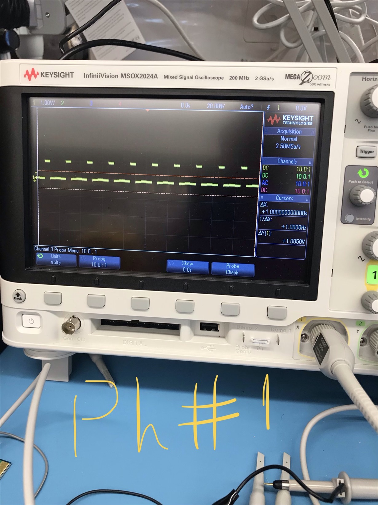
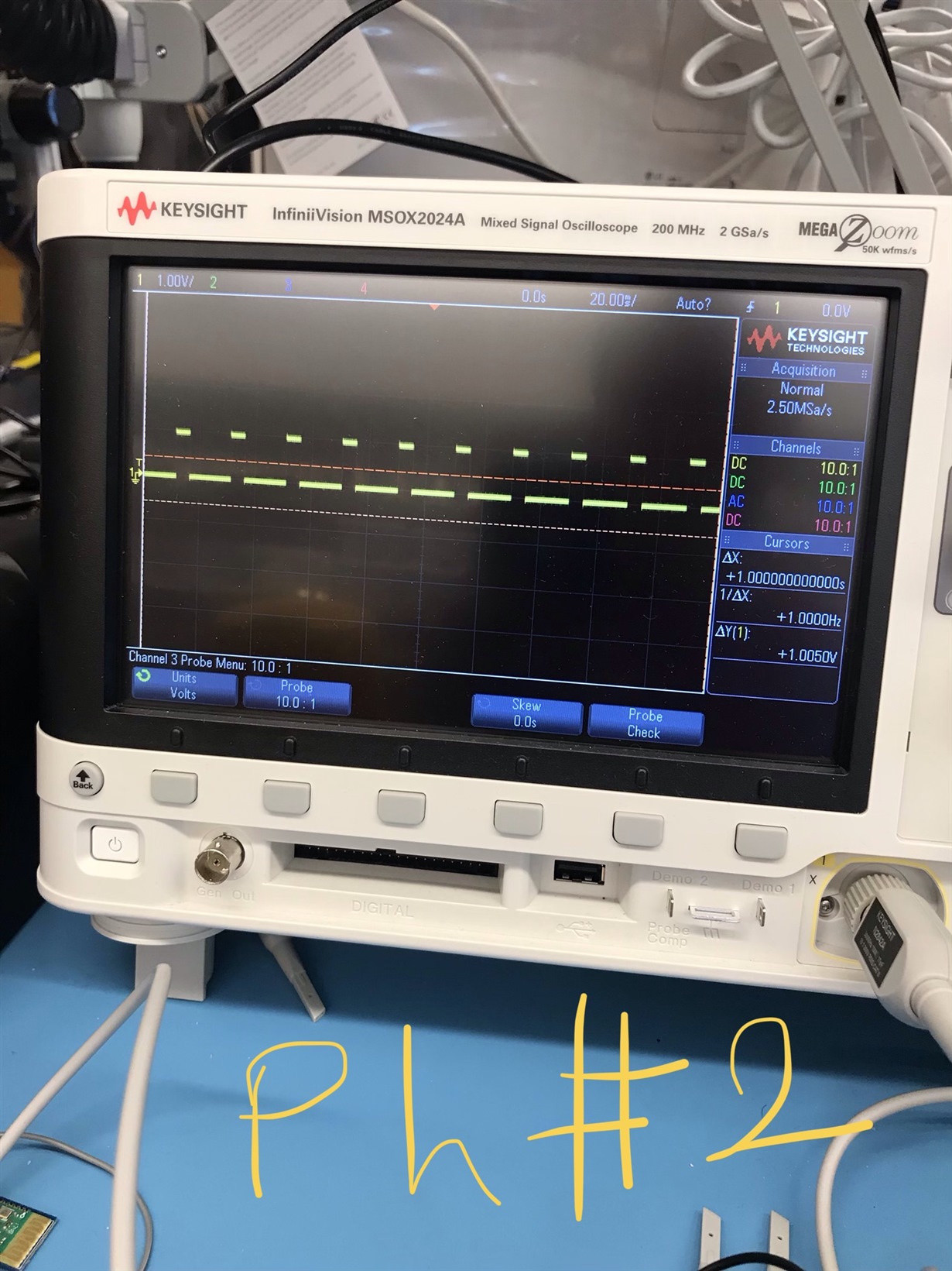
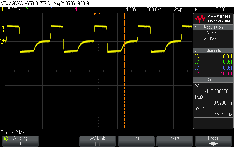
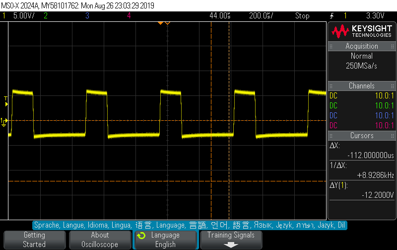
  • I am sorry I couldn't comment near the pictures. But my input signals are square waves like in the pictures as phase 1 and 2.

  • Hi Alpaslan,

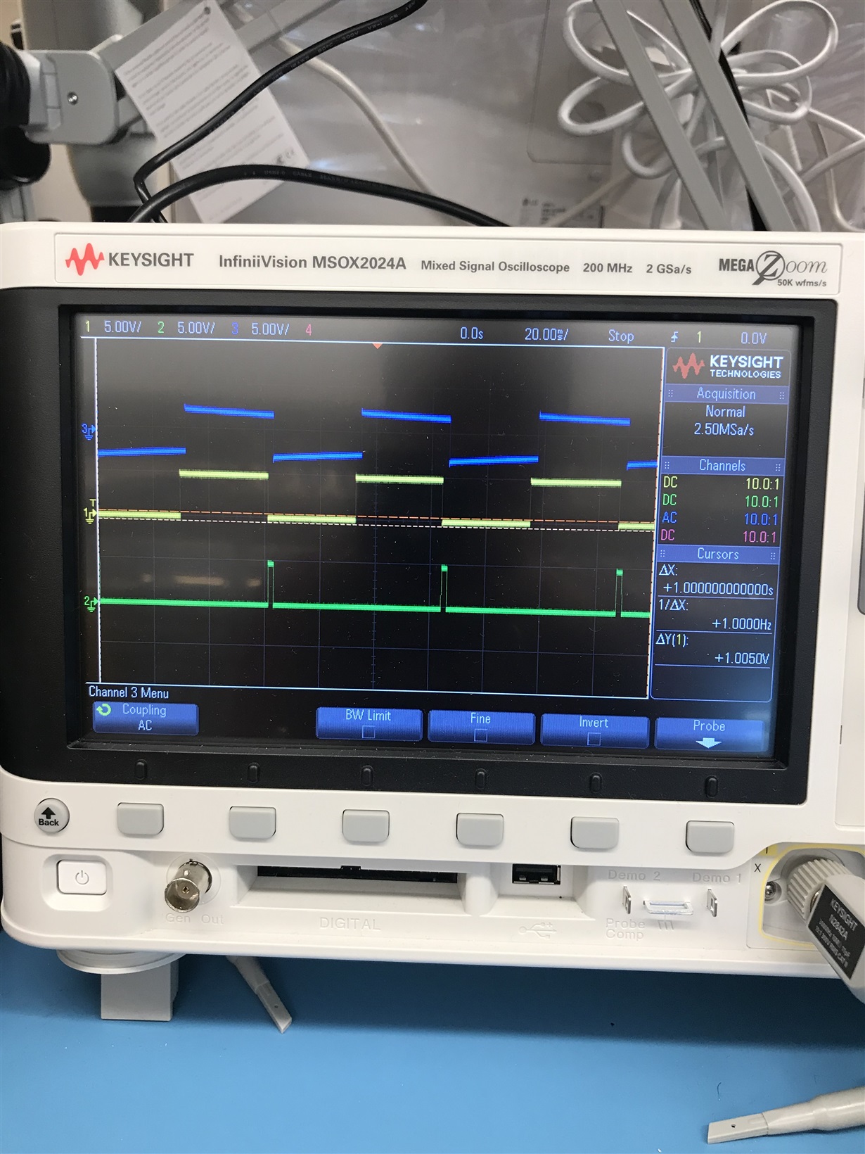
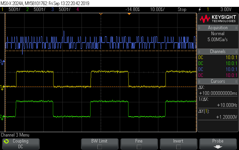
    Can you provide a scope shot showing Phase 1, Phase 2, and the output all on one measurement (using 3 separate scope probes)? This will help us see what the issue might be.

    Thank you,

    Tim Claycomb

  • Hello,

    Of course! I attached the all signal outputs. Blue:Phase 2; Yellow: Phase 1; Green;Output.

  • Hi Alpaslan,

    are you sure that -5V is connected to pin 4 of TLV27L1?

    Kai

  • Hi Alpaslan,

    Have you verified that the -5V supply is connected as recommend by Kai?

    Thank you,

    Tim Claycomb

  • Yes, it is connected. I will make a new design. Can I use TLV2371IDR instead of the current one? With this new IC, can I get more stable signal?

    Because in the olde one, it works properly. After somehow I lost the signal. It happens many times before. The reason can be related with supply voltage symmetry? 

  • Hi Alpaslan,

    The supply voltage symmetry should not matter. As long as there is a total supply voltage within the specified supply voltage in the datasheet for the device, and there is enough supply voltage for your required output voltage, then everything should work as expected (provided there is nothing else being violated in the datasheet).

    Does the supply voltage ever drop out?

    Are you using a bread board to verify your design or soldered down components on a PCB? If you are using a breadboard make sure all connections are solid, if you are using a PCB make sure you do not have any cold solder joint or lose connections.

    Regarding your question on if you can use the TLV2371, there should not be an issue but it has significantly higher power than the TLV27L1. If you provide me with a list of specifications (Bandwidth, Iq, Offset Voltage, Supply Voltage, Input voltage, etc.) I would be happy to make a device recommendation for you.

    Thanks,

    Tim Claycomb

  • Thank you!

    "Does the supply voltage ever drop out?" 

    At the end of my tests, I close the power of the PCB with shut down switch manually. Do you think this cause a problem?  

    Supply voltage +5V and -5V. Input signals are square waves and their amplitudes are adjustable. I don't have information about bandwith, Iq and offset voltage.

  • Hi Alpaslan,

    do not apply any input signal to the TLV27L1 when the OPAmp is not powered.

    I would take a fresh TLV27L1 and test again.

    Kai

  • Hi Alpaslan,

    I agree with Kai. Replace the device and test again. Always turn off the input signal before powering down the device.

    Thank you,

    Tim Claycomb

  • Hi Alpaslan,

    Did replacing the device with a new unused device solve the problem?

    Thank you,

    Tim Claycomb

  • Hi Tim,

    Thank you for asking! No, it didn't solve it. I erased the microcontroller for not supplying an input signal to the OpAmp. Then I solder a new OpAmp on the board and test it. But the problem remains on the board. My plan is to solder a new PCB and test it. 

    In my project, the output signal of the opamp flows to inputs of the individual 32 SPST switches. The problem occurred when I solder 7th and 8th switch IC. Before that everything has worked fine.

    Thank you,

  • Ok. Let us know if you need any additional support once you get your new board up and running.

  • Hi Tim,

    I have a question. I feed square waves to the both inputs of the OpAmp. I measure the square waves before the 50k resistors but after the 50k I lost the square wave signals and get 4V step function signal. For example, when I change the amplitude of the square waves, I always get 4V signals every pin of the OpAmp except power lines.

    What this problem occurs?

    Thanks,

  • Hi Alpaslan,

    The voltage that connects to the non-inverting input (pin 3) is only a voltage divider. So at pin 3 (the non-inverting pin) you should only see an attenuation (two thirds) of your input signal (phase 2). Unless of course something is wired incorrectly or broken. Do you always see a 4V signal on pin 3 (at the R30/R31 node)?

    Thank you,

    Tim Claycomb

  • Yes, there is 4V after the 50k resistors at non-inverting and inverting inputs. 

    Now, I have just solved the problem with refreshing the OpAmp. This part is really important in my design because of that I try to understand the source of the problem. Do you recommend the go-ahead with the same OpAmp or do you suggest any more efficient OpAmp than this?

    This OpAmp output connects to 16 analog switches inputs. So multiple analog switches cause any loading effect than the OpAmp goes error? So do you recommend multiple OpAmps to generate the same signals?  Or different OpAmp?

    Thank you,

  • Hi Alpaslan,

    It depends on what is causing the damage to your device. If you are not using ESD protection while handling your PCB and devices then the damage may be coming from ESD. If it is something like an overvoltage on the input then you will need to ensure the device is properly protected.

    I'm not sure I understand the second set of questions. Can you explain in a little more detail (or provide block diagrams/schematics/etc.) what you mean by "So multiple analog switches cause any loading effect than the OpAmp goes error?" and "So do you recommend multiple OpAmps to generate the same signals?"?

  • I see, actually, I try to be careful about ESD protection. I use ESD tweezers and ESD mat during working on the circuit.

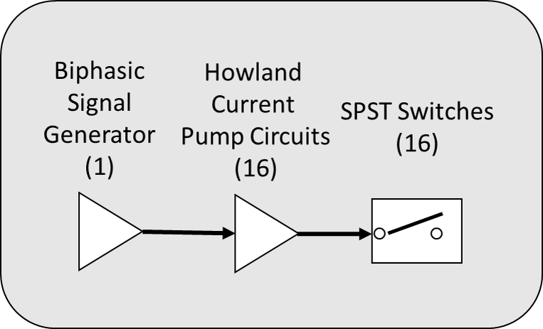
    For clarification to my questions, I share the block diagram.

  • Just to ensure I understand your question correctly. Are you asking, should you use the same op amp (TLV27L1) for the biphasic signal generator and howland current pump circuits?

  • If the TLV27L1 can meet all the requirements of your howland current pump circuit then I do not see a reason to use a different op amp for your design. However, I see that the maximum output current of the TLV27L1 is only a few milliamps. So if you require amps of current out of your howland current pump you may need to use a different op amp.

  • Actually, I plan to get 100uA level outputs from each of the Howland pumps. For example, if I activate 16 switches and the pumps at the same time, this OpAmp may not enough supply signals, isn't it? So what is your suggestion as more output current OpAmp?

  • Hi Alpaslan,

    I think if you only need 100uA from each amplifier you can use the TLV27L1 for all op amps. I recommend taking a look at this app note that discusses the Howland Current Pump to make sure you design a circuit to meet your needs.

    Thank you,

    Tim Claycomb

  • Hi Tim,

    Thank you for your reference!

    I designed a Howland current pump circuit and simulate in the TINA TI which is attached as a simulation and screenshot files. I fed to the top opamp with 2V step function signal. Actually I tried to feed with biphasic signal but I couldn't find in Tina TI. So, I have two questions:

    1. I calculated output current from Howland Current pump as 2V/25k= 80uA, but I measure as 2V from amperemeter. Is there a problem in the configuration and meter position?
    2. Do you recommend anything about the design and resistor value selection? Based on my readings, R1/R3=R2/R2 with high precision. My resistors on my board have 0.1% and 1% precisions. 

    Thank you,

     howland.TSC 

  • Hi Alpaslan,

    There were a few wires that did not get connected in the schematic your provided. The wire from R3 to the output was not connected and the wire connecting the volt meter on the output of U1 (VM1).

    Try the attached schematic and let me know if it works for you.

    howland_TI Edits.TSC

    Thank you,

    Tim Claycomb

  • Thank you TIm!

    I measured as 20uA from AM1. The current flowing through 100k resistor is depending on the R5 resistor value, isn't it? The other thing is that R2 and R4 have 1% tolerance and R1 and R3 have 0.1% tolerance. Does this difference cause any problem with the balance of resistor ratios (R1/R3=R2/R4)? 

  • Hi Alpaslan,

    The current through AM1 is input voltage/R1 = 0.5V/25k = 20uA.

    Can you make the resistance tolerances equal? Not having a equal tolerances will likely cause an increase in error.

    Thank you,

    Tim Claycomb

  • Thank you! 

    I will take a look the same tolerance resistors.

    The other thing is that when I double check your TINA design, I revealed that you connected source as in input. I switched to the voltage generator and set the biphasic signal pattern and 2V amplitude. When I do this modification I measure -39.86uA on the AM1 so why I get this value? 

  • Hi Alpaslan,

    With a 2V input the output of the op amps are slammed to the rail (-5V). You cannot have over a 1V input with the gain configuration you have. Trying sweeping the input voltage from 0V to 2V and you will see that VM1 slams to -5V with a 1V input. You can run a DC sweep by going to Analysis => DC Analysis => DC Transfer Characteristic.

    If you require a 2V input increase resistors R1 and R2 in your circuit to 50k ohms.

    Thank you,

    Tim Claycomb

  • Hi Tim,

    When I do the DC characteristic analysis, if I understand correctly, the opamp goes to the saturation with 2V inputs. So I can adjust or control the input voltages. My target is that +/- 30uA biphasic current signal. So I will apply +/- 1V biphasic signal as an input to inverting side of the opamp, then I will get 1/34k=30uA biphasic current signal with amperemeter. Is it true? And also, how can I visualize the current waveforms in the program? 

    Thank you,

  • Hi Alpaslan,

    Yes you are correct. Having a 2V input will saturate the output of the op amp.

    The last schematic that was provided showed a 25k ohm resistor for R1 so the output current with a 1V input would be 1/25kohm = 40uA. If you want 30uA with a 1V input then you would need to change resistors R1 and R2 to 34k ohm like you have mentioned above. You will just need to make sure that having a 34k ohm resistor will not cause the output voltage to saturate.

    I'm not sure I fully understand your question "how can I visualize the current waveforms in the program?" The current is measured using AM1 in the TINA file you provided. AM1 will provide the current through the load for both DC and Transient simulations. Is this what you meant by your question?

    Thanks,

    Tim Claycomb

  • Yes, I have selected R1=25k; R2=5k; R3=34k; R4=6.08k. I think 34k is fine for my case, am I right?

    You are right about ameperemeter. 

  • Hi Alpaslan,

    Choosing those component values will cause the op amp output to rail again. Attached is a TINA file that outputs 30uA with a 1V input. Please let me know if this will work for you.

    howland_TI Edits_2.TSC

    Thank you,

    Tim Claycomb

  • Hi Tim,

    Actually, I didn't understand the meaning of the 'goes to rail'. Does it mean saturation? Why the selected values are not working? In the Howland pump, the ratio is not only the key point?

    Thank you,

  • Hi Alpaslan,

    "Goes to the rail" means the output has reached the largest output voltage it can possibly get to or "saturation".

    The reason using R1=25k; R2=5k; R3=34k; R4=6.08k does not work is because the gain of this circuit causes the output voltage to saturate before it reaches the 30uA output current.

    Correct, the ratio of the input voltage and input resistor is not the only key point. You must ensure that the op amp stays within its linear operation. I recommend watching out TI Precision Lab Videos on Input and Output Limitations for more information. There is also a lot of other helpful information in the other videos.

    Thank you,

    Tim Claycomb

  • Thank you, Tim! They are really helpful videos. I watch them.

    But I couldn't still figure out. When R1:25k; R3:5k; R2:34k; R4: 6.8k, the output voltage is -4.984V at pin 1 of the U1 opamp so it exceeds the low output voltage range (-4.95V or -4.84V). V+ has -4.154V and V- has -3.987 so common-mode input voltage range is -0.167. In the datasheet, the range is 0 to 3.65V so the common voltage also is out of the range.

    In your case, R1:34k; R3:5k; R2:34k; R4: 5k, the output voltage is -4.987V at pin 1 of the U1 opamp so it exceeds the low output voltage range (-4.95V or -4.84V). V+ has -4.348V and V- has -4.219 so common-mode input voltage range is -0.129. In the datasheet, the range is 0 to 3.65V so the common voltage also is out of the range.

    In your design, the voltage source looks like a step function signal. But I expect to feed with biphasic square signals.

    Thank you for your help! I really learn many things through these conversations.

    So, could you explain a little bit more detail why your case is true?

  • Hi Alpaslan,

    The reason the inputs are not equal is because the output is saturated to the negative rail. If the output is not saturated, the op amp is able to "regulate" the inverting input pin. The common mode voltage range is from V- (-5V) to V+ (+5V). Please see section 7.2 in the datasheet. The reason section 7.2 states the common mode voltage is from 0V to Vdd is because it assumes single supply operation. But if you use dual supply operation the common mode voltage is from V- to V+.

    With R1:34k; R3:5k; R2:34k; R4: 5k the output does not saturate. It outputs -3.52V with a 1V input. Please see below.

    Thank you,

    Tim Claycomb

  • What do you think about this?

  • Hi Alpaslan,

    This looks much better. The output voltage is now in a linear region with the maximum input voltage. The only other thing I recommend testing is to apply a signal that is similar to your actual input signal just to make sure everything operates as expected.

    Thanks,

    Tim Claycomb

  • Hello,

    Now my howland current pump works with biphasic voltage. I have three questions.

    1. I didn't connect any load as an output of the howland current pump. I measure the current signal with oscilloscope probe. Do you think is it right approach or should I connect a resistor then measure voltage across it?
    2. I want to examine the current signal measured as a voltage with my probe. I know why the phases are not symmetric because the resistor values are not matched and tolerances are different in the previously designed howland circuit. The curve which goes negative to zero is capacitor (0.33uF) discharging, isn't it? Do you have any other comments about the signal.


                    3. My last question is about an error. From three different channels, I didn't get the exact signals what I have in the second question. So where should be a problem? I check the microcontroller outputs and switches and all of them work. I guess the problem is in the howland pump part. What is your suggestion about solving the problem?


    Thank you,

  • Hi Alpaslan,

    Current outputs need a load in a similar way that a voltage source shouldn't be shorted. You can use a low value resistor and measure voltage or you can use a short and a current probe. The resistor has to be low enough so that the voltage is within the compliance range of the current pump. 

  • Ok, thank you!

    One more question. When I measure signal after a resistor (R1=25k in TINA TI design in previous posts) which at inverting input of the opamp, I get this signal which is attached this post. But when I measure another howland pump configuation, I didn't get same signal at same node. The measured signal is just zero. Why is that happen?


  • I have just solved the problem couple of minutes ago. 

    I check one by one each of the component with a SMD tester (http://www.mastech-group.com/products.php?cate=104&PNo=76). I realized that R2 resistor value supposed to 34k but I measured 20 Ohms. So I removed the component and check the its pads. I found that there had been a short circuit between of them. When I double check the layout, GND connection makes a short circuit a trace which is connecting R2 to noninverting input of the OpAmp. Hence, I broke the trace and solder a jumping cable according schematic design.

    Actually I did this design with Altium. I run design rule check before the fabrication and the program didn't report any short circuit. 

    Anyway, thank you for your support!

  • Alpaslan,

    Good work; glad you found and fixed the problem.

  • Hi Ron or Tim,

    In this thread, you will see very first opamp circuit. I feed 20us pulse width signals to the inputs of the opamp but I didn't get a meaningful signal as an output. Blue is output signal; green is phase 1; and yellow is phase 2. So how can I get a true signal as an output?

    Thank you


  • Alpaslan,

    The first schematic is a difference amplifier. With both inputs being the same, the output should be zero.