This thread has been locked.

If you have a related question, please click the "Ask a related question" button in the top right corner. The newly created question will be automatically linked to this question.

THS4001: Output voltage is 0.5V greater than the expected voltage with composite architecture.

Part Number: THS4001
Other Parts Discussed in Thread: TLC2652,

Hi,

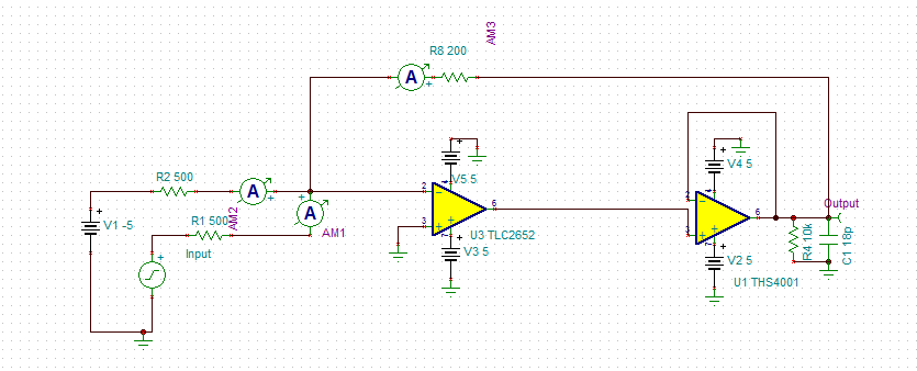
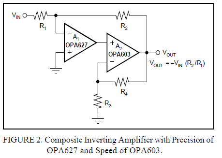
I am using the composite opamp with TLC2652 (chopper stabilized opamp) and THS4001 (High speed opamp).

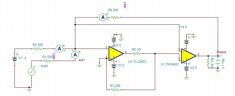
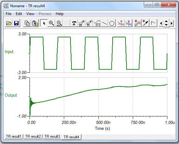
If the input voltage is -5V from the battery V1 without the AC input, the expected output voltage is 2V since the gain of the circuit is 0.4.

I was able to measure the 2V if a decap of 6.8uF (polarized) is not added for THS4001 opamp power supply pins.

I am using a parallel combination of 0.1uF(ceramic) and 6.8uF (tantalum) at the power supply pins of THS4001.

With these two as decaps, my output voltage is 2.5V but with only 0.1uF decap, i am able to measure 2V.

What might be the reason for this condition.

Note: For TLC2652, only 0.1uF (ceramic) decaps are used.

Thanks

Pavithra Joshi

  • Hi Pavithra, 

    I'm not really sure how to best analyze the circuit you've shown in the diagram. I'm not sure if this circuit will actually function properly as a composite loop because the summing junctions are being shared by both of the amplifiers. I am also concerned by the positive feedback connected to the TLC2852 causing an oscillation. I would suggest that you follow one of the standard composite configurations shown in the following application note. 

    http://www.ti.com/lit/an/sboa002/sboa002.pdf

    Regards, 

  • Hi Jacob,

    Thanks for suggesting that application note.

    Can you please help me with the chopper stabilized opamp which is being planned to use it in the composite architecture.

    The TLC2652 chopper stabilized opamp has the block diagram showing the external capacitors Cxa and Cxb are connected to VDD-.

    I want to know why it is connected to VDD-.

    Thanks

    Pavithra Joshi

  • Hi Jacob,

    I tried the composite configuration suggested by you in simulation.

    Expected output is square waveform which was not achieved in the output.

    Thanks

    Pavithra Joshi

  • Hi Jacob,

    I also tried shirting the inverting input of the THS4001 to the inverting input of the TLC2652. 

    I am getting the proper output as expected.

    Please help me whether this can be implemented or not.

    Thanks

    Pavithra Joshi

  • Hi Pavithra, 

    I believe the reason the composite circuit did not work for you is because you appear to be using a 5MHz signal but the TLC2652 is only a 1.9 MHz amplifier. If you use a higher bandwidth amplifier, then you should be able to see the signal properly. Your second circuit is working because you are directly driving the summing node of the THS4001, which will remove the precision benefit of the chopper amplifier. 

    Regards, 

  • Actually, this 2nd composite might work - the chopper will take control of the final DC output level - there will be a long electrical settling tail as the slower device takes over the output control. There also might be some stability issues as the 4001 adds prop delay inside the loop of the chopper, so you should check that - an output spot noise sim is a quick way to do that.Go out to 100MHz and look for a spike in the spot output noise

  • Hi Jacob,

    I actually referred an old article related to the composite amplifiers and followed the same circuit they had suggested.

    I actually read the article suggested by you from TI for the composite opamp architecture and found that the slew rate and precision are achieved based on the R3 and R4 resistors.

    I didn't find how the values of resistors are selected. Please help me to learn the same.

    Thanks

    Pavithra Joshi

  • Hi Michael,

    As suggested, i tried for the noise analysis for the composite architecture.

    Below is the output noise and total noise curves for the same.

    I cant find any spikes in the curves. 

    Also the total noise at 1MHz frequency is 21.32uV.

    Can you help me understand this analysis.

    Thanks

    Pavithra Joshi

  • Hi, 

    R4 is chosen based on a reasonable value for the amplifier and then R3 is set by the equation on page 2 

    R3 = R4 R2/(2 • R1)) – 1

    Regards,