This thread has been locked.

If you have a related question, please click the "Ask a related question" button in the top right corner. The newly created question will be automatically linked to this question.

INA213: INA213AIDCKR Field Issues

Part Number: INA213
Other Parts Discussed in Thread: TPS7A4001

Hi TI Team,

Need Urgent help,.

We are Using INA213AIDCKR in our Design, we are seeing many random failures in our board due to this device.

Number of failures are increasing day by day.

We have observed that Vref(2.5V) which we are giving to the Ref pin has changed in all the field failure returned Boards.

Currently we are providing Reference voltage(2.5V) through voltage divider circuit,10 is attenuated to 2.5V through 30k & 10K resistor.

And  we observed that reference voltage is changing when sudden interruption of corruption through resistance(100uOhm). Reference voltage is changing from 2.5V to 18V.

We also observed that after the IC is de-soldered & soldered it back sometimes IC is again working fine. I am suspecting during desoldering & soldering because of the high temperature during de-soldering & soldering the property of silicon might be changing.

Kindy help us to solve this issue urgently, Field issues are increasing everyday & we have deployed more than 1500 boards in the field across multiple customers.

Kindly do the needful.

  • Hi Yogesh,

    have you protected and filtered the inputs of INA213? Are you sure that the maximum input voltage has never been exceeded?

    Are you sure that the PCB was soldered properly? Was the flux totally removed after soldering?

    By the way, the reference voltage should not be supplied by a resistive voltage devider without buffer stage. This can ruin the common mode rejection of INA213.

    Can you show a schematic?

    Kai

  • i Kai,

    Thanks for your reply.

    We have not added any protection diodes & but we have added series resistor & filter capacitors on the input lines for (IN+ & IN-)

    Yes I know Reference voltage should not be given directly but this design was initially reviewed by TI if I am not wrong(I can check internally this).

    Yes PCB was soldered properly, INA213 in all boards were working fine but over time (after 1 to 3 months of time in field) this IC is malfunctioning.

    I am thinking during de-soldering & soldering the IC back on board because of high temperature Silicon properties might have changed & IC is working fine afterwards. I am not able to clearly understand what could be the reason why IC is malfunctioning after sometime.

    I have attached schematic section, kindly review it.

  • Hey Yogesh,

    I have been working on this issue off-forum, but thanks for providing information.

    My best understanding currently of this issue is:

    • Board failure occurs after 1-3 months
    • Failure mode is that Vref is measured at around ~0.5V, when it should be 2.5V.
    • If broken INA213 is removed, then the Vref node turns into 2.5V.

    As for the last point about the de-soldering and re-soldering the same device I would like some more information about this test:

    1. Are you performing this test on boards that were returned from the field or failed in-house tests?
    2. Were these broken boards ever powered-down and then power-up and then re-tested before the INA213 was removed and repopulated?


    There should be no difference between powering the system down and removing & repopulating the device. I don’t see any reason why de-soldering & re-soldering would change the behavior/silicon of the device unless there is an internally latched ESD cell, but if there was, then powering down and powering-up would unlatch the ESD cell as well. Please make sure that any broken boards are powered-down completely before testing again. Of course make sure any re-worked boards are cleaned and free from flux residue before testing again.

    Here are some more questions.

    • I was informed that in-house tests show that a current transient in the load is reproducing the failure? Am I correct in thinking this?
    • Would you please provide a waveform, if possible, on what the voltage at the input pins (IN+, IN-) looks like during the current transient?
    • Which version of the INA213 are you using (A, B or C version)?
      • Please consider testing with the B or C versions. They have better ESD immunity and these failures are probably due to a ESD latch up at the input pins of INA213.      
      • What is supplying the 10V rail?
      • Could you measure the current going into the REF pin (pin 1) of device for a failing system? You could measure this by measuring voltage drops across the 30k and 10k and subtract the currents: IREF = VR38/30k – VR41/10k.

    Hope this helps and that we can solve this issue quickly.

    Best,

    Peter

  • Hi Yogesh,

    I think, that if the chips work again, after desoldering and soldering back onto the PCB, they had not been soldered properly at the beginning. 

    Nevertheless, I would add some common mode noise input voltage filtering (caps from each input to GND). Why not using the suggested circuitries of figure 27 and 29 of datasheet? Combine both circuitries and your inputs are absolutely safe!

    Kai

  • Hi Peter,

    Thanks for detailed response.

    Regarding your queries.

    1). Not in all boards after removing INA213 & putting it back IC is working but I have seen in 3 boards out of 4 boards  IC was working fine after de-soldering & soldering it back.

    2). Boards were completely powered down &powered up again, still the issue was same. We did this multiple times.

    3). Only after removing IC & putting it back at least in 3 boards I saw Vref  is as expected.

    4) We saw the Vref was shooting up to 18V even through supply voltage to resistor divider net work is 10V. but what I observed is overall voltage across resistor network remains same but when Vref was shooting up I saw Voltage across 30k is dropping & Voltage across 10k is increasing, so the overall voltage across resistor network remains 10V.

    From this what I understood is Ref pin of INA213 is sourcing current to 10K resistor.

    5). We are using INA213 A version.

    6). we are powering the INA213 from 10V LDO(TPS7A4001).

    7). I have tested with C version of INA213 also & the behavior of Vref remains same. I am really not sure is this overshoot of Vref can be the reason for IC to malfunction. 

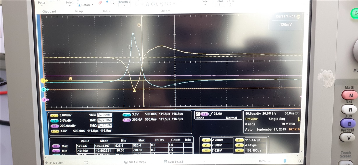
    8).  I have attached the voltage across 30k & 10k during transient event happened at the time of opening the MOSFETs.

    Blue is voltage across 10k & yellow is voltage across 30k. (Sorry picture quality is not good, I took it from my mobile due to urgency)

  • Hi Kai,

    Thanks for your response.

    If soldering was the issue then IC was working fine initially for long time. We are seeing issue after 1 or 2 months of operation,

    Yes we can improvise the design, but we need some quick solution without not modifying any circuit. ( because changing design takes some time & we have as I informed earlier we have already deployed more than 1500 boards.

    So I am looking for quick easy solution as ICA. If INA213 B & C version can solve the problem then we can quickly implement at least in new production boards.

    Regards,

    Yogesh

  • Hey Yogesh,

    Thanks for the scope shot, but I do want to confirm that you probed across the 30k resistor with a differential probe, correct? A single-ended probe that is connected to the oscilloscope’s board ground will pull down REF to 0V.

    It is important that we try to establish a connection between the Vref rise and the device failure.

    Would you please perform the same test, but probe IN+, REF, OUT and Vs during the time of opening the MOSFETS (transient event)? This will help me determine the root cause of INA213 damage.

    Sincerely,

    Peter

  • Hi Peter,

    I am not sure whether VRef rise will damage the IC or not but I felt this might be probably reason why INA213 is failing or malfunctioning after some time.

    And yes we have taken the voltage across 30k & 10k using a differential probe only.

    We will try to take ones again one more measurement with all the test points which you have requested.

    but I wanted to understand can the Vref rise cam damage the IC.

    Thanks

    Regards,

    Yogesh

  • Hey Yogesh,

    Yes. A rise in Vref (voltage at REF pin with respect to INA213's GND pin) can certainly damage the part. In order to determine what the limits are for REF or any other pin refer to the Absolute Maximum Rating table in the datasheet. Violating any of these conditions can damage the device.

    So if VS is at 10V and Vref rises to 18V even for a brief period of time, then this can damage the device. However, we need to be certain that the GND pin is not also moving. In other words we need to be sure that the ground of the system and ground of the INA213 are always the same potential. This is usually the case, but sometimes if there is along trace with inductance connecting these grounds a potential difference can occur. This could make certain pin voltage measurements misleading.

    Additionally, the REF pin could be rising due to voltage transients at the IN+ and IN- pins and this is why I ask for those to be probed as well.

    Thanks for working with me on this. I hope we can solve this in a timely manner.

    Best,

    Peter

  • Hi Peter,

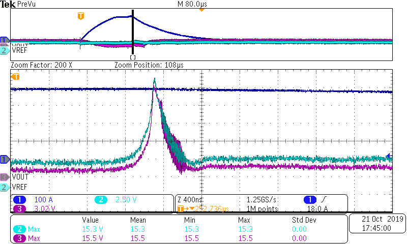
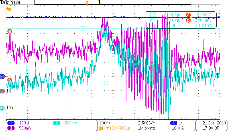
    Please find the waveforms of Vref, Vout, IN+, IN- measured using differential probe.

    It seems dv/dt is very high & also Vref was shooting up to 15V( we have seen up to 18V).

    Kindly let us know if any more information required.

    Regards,

    Yogesh

  • Hey Yogesh,

    Thanks for the waveforms.

    • Why is IN- voltage higher than IN+? Was this just a temporary condition during the load transient?
    • Is IN- pin connected to board ground as it is in most low-side applications?
    • A schematic and picture of the PCB layout would be helpful. This can be sent privately to my email.

    I'm looking this over with my team, but there is some very high-frequency ringing at the input and this must cause the REF pin voltage to rise since the 10V rail seems to be stable based upon earlier messaging. Although it remains to be seen if this load transient event is what is actually breaking the devices. All measurement should be taken with respect to the INA213 GND pin as there could be a difference between system ground and INA213 GND. The schematic and PCB layout photos should help rule this out.

    Sincerely,

    Peter

  • Hi Peter,

    a. IN- is greater bcoz IN- is connected to other end of the shunt & IN+ is the battery ground which is same as INA213 ground.

    b. IN- pin is not connected to board ground, IN+ is connected to board ground.

    c. Yes all measurements are done with INA213 ground only.

    Kindly share your email id so I can share it with you schematic & PCB layout.

    Thank you.

  • Hi Yogesh,

    as your input signals seem to go negative and to violate the absolute maximum ratings, you urgently need to improve your ground routing! And, even if I repeat myself, I would strongly recommend to add some common mode noise input voltage filtering (caps from each input to GND). Again, why not using the suggested circuitries of figure 27 and 29 of datasheet? Combine both circuitries and your inputs are safe.

    Kai

  • Hey Yogesh,

    Sorry. My email is p-iliya@ti.com

    Just to make a comment about Kai's suggestion. Input common-mode caps from IN+ to ground and IN- to ground would slow down the fast VCM transients, but there are two tradeoff: load capacitance and reduced accuracy to load step responses. So if the load current jumps from one level to another quickly, the INa213 with input RC filters will have a slower settling time. This is because the input RC filter for each input pin will have different time constants due to capacitor tolerance mismatch. Imbalance time constants will lead to different charging/discharging times, and this will create a dynamic input offset that will need to discharge after a load step response.

    Best,

    Peter

  • Hello Yogesh, Peter, Kai,

    I am closing this thread since support has been moved to direct e-mail. Peter, if any useful debug tips can be posted here once the root cause is found, please do so.

    Best regards,

    Ian Williams
    Applications Manager
    Current Sensing