This thread has been locked.

If you have a related question, please click the "Ask a related question" button in the top right corner. The newly created question will be automatically linked to this question.

INA333: INA333 offset voltage

Part Number: INA333
Other Parts Discussed in Thread: ADS1262

Dear Responsible;

In our prototype design we have used INA333 for thermocouple measurement circuits. Gain is set to 1 by not populating R104

When the inputs of the INAMP is shorted @+&- inputs; difference between REF&OUT means offset voltage is about 12mV which is inconsistent with the datasheet value of ~100uV with Gain=1?

Do you have any idea or comments?

Best regards  

  • Hi Ilhan,

    It appears you are biasing the thermocouple at the middle of +Vbias/-Vbias supplies; outside the input common-mode voltage range of the INA333 instrumentation amplifier.

    On your schematic, the thermocouple voltage is biased between +Vbias and -Vbias. If the +Vbias/-Vbias supplies are symmetrical positive/negative supplies, the differential thermocouple voltage is centered at a common-mode voltage of VCM=0-V. 

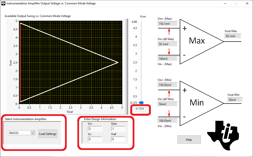
    Please note, the allowed INA333 input common-mode voltage range is a function of the INA333 supplies (V-, V+), the REF voltage, the gain, and the INA333 output voltage.  Please refer to Figure 21 p.10, and section 7.4.2 p.13, to read about the INA333 valid common-mode voltage range vs output voltage. You can also use the Instrumentation Amplifier Common-Mode Voltage Calculator to estimate the valid common-mode voltage range of the INA333 for different supplies, reference voltages and gain configurations.

    On your circuit, when using the INA333 with V+=+5V, V-=0V, REF=0-V and Gain=1; the minimum allowed input common-mode voltage is positive +0.125V; and therefore the thermocouple common-mode voltage its outside the linear input range of the INA333.  See below common-mode voltage range using the Instrumentation Amplifier Output Voltage vs Common Mode Voltage Calculator :

    You may download the Common-Mode Input Range Calculator for Instrumentation Amplifiers on the link below:

    http://www.ti.com/tool/INA-CMV-CALC 

    A possible solution is to change the thermocouple VBIAS voltage so +Vbias = +5V and -Vbias = 0V.  This will set the thermocouple common-mode voltage right at the center of the INA333 supplies, inside the instrumentation amplifier common-mode voltage range. 

    Thank you and Best Regards,

    Luis


  • Dear Mr. Chioye;

    First of all thank you for your prompt reply.

    today i was very tired and confused due to this circuit, sorry, i forgot to say that in my design +Vbias = +5V and -Vbias = 0V and Vref is coming from ADS1262 ref voltage which is 2.5V. In summary the values exactly the same as your recommended settings.

    (since this is a prototype i will try to test Excitation voltage switching, commonly used for RTD type circuits. I just want to see this chopping effect for long cable thermocouple design)

    As a reference I used directly REFOUT pin of ADS1262 in one option and AIN COMMON pin in the second one. From ADS1262 datasheet AIN COMMON pin has 100R output impedance so in the second round i tried the direct REFOUT of ADS1262. But the result was the same, nearly 12mV output@shorted inputs.

    The test equipment is 5 digit DMM, a special tool from Fluke.

    What is your recommendation?

    Regards

  • HI Ilhan,

    Is there any capacitive / RC load driven by the INA333 output prior to the ADC on the circuit above?  I would like to verify the stability of the INA333 driving the RC filter.  Also, when measuring the INA333 output with the external meter, are you applying the meter cable/probe after the filter series resistor? 

    In your test where the INA333 Inputs are shorted, please verify with the external meter that the inputs are set to the expected ~2.5V common-mode and 0-V differential?  I am assuming this test was performed using static voltages for initial debug.

    If possible, please provide the complete schematic showing the ADS1262 connections.

    Thank you and Regards,

    Luis

  • Dear Mr. Chioye;

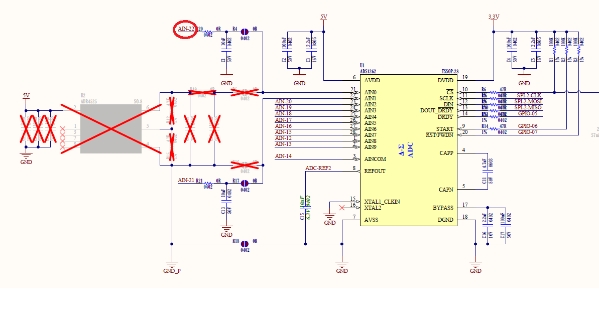
    There is only 0R and 10nF on the ADC way,

    during measurement i just probe at INA333 OUT and REF pins. Inputs were shorted just right IN+ and IN- pins.

    Below you can find ADS1262 schematic

    Best regards

  • HI Ilhan,

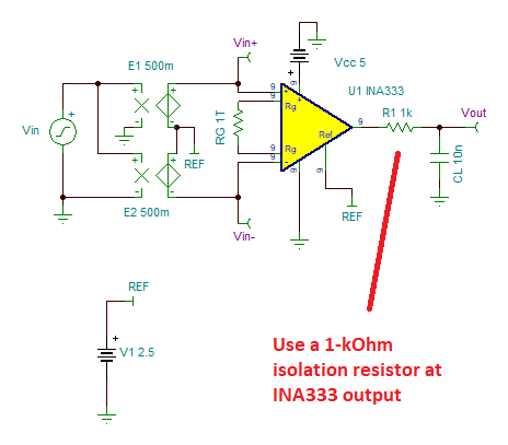
    Most amplifiers can become unstable while driving large capacitive loads; and the INA333 output will be unstable driving the 10-nF load directly.  I recommend you replace the 0-ohm resistor between the INA333 and the 10nF load with a 1-kOhm resistor to isolate the capacitive load. 

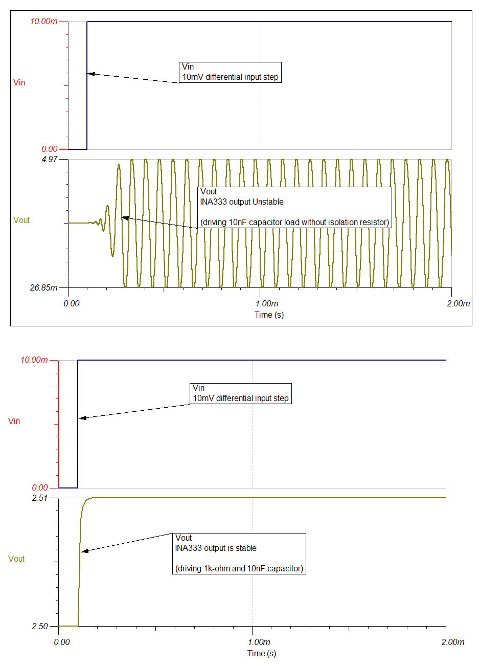
    Below is the TINA simulation results of the INA333 driving (a) 0-Ohms + 10nF  and (b) 1-kOhm+ 10nF.

    The transient simulation shows the INA333 output can oscillate after a 10mV input step when using 0-Ohm +10nF.  In contrast, the transient output response is stable result when using 1-kOhm+10nF RC load. 

    See recommended circuit and simulation below. 

    Thank you and Best Regards,

    Luis