Other Parts Discussed in Thread: OPA858, OPA855,
I've had in this evaluation board and a blank for testing the OPA858 and OPA855, and my bench tests have been returning consistent results, but not the results I was expecting from what I've gathered off the component datasheets.
Attached are some of my experiment results, along with a photograph of my test setup.
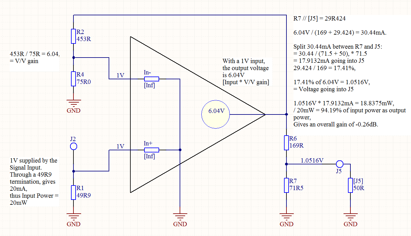
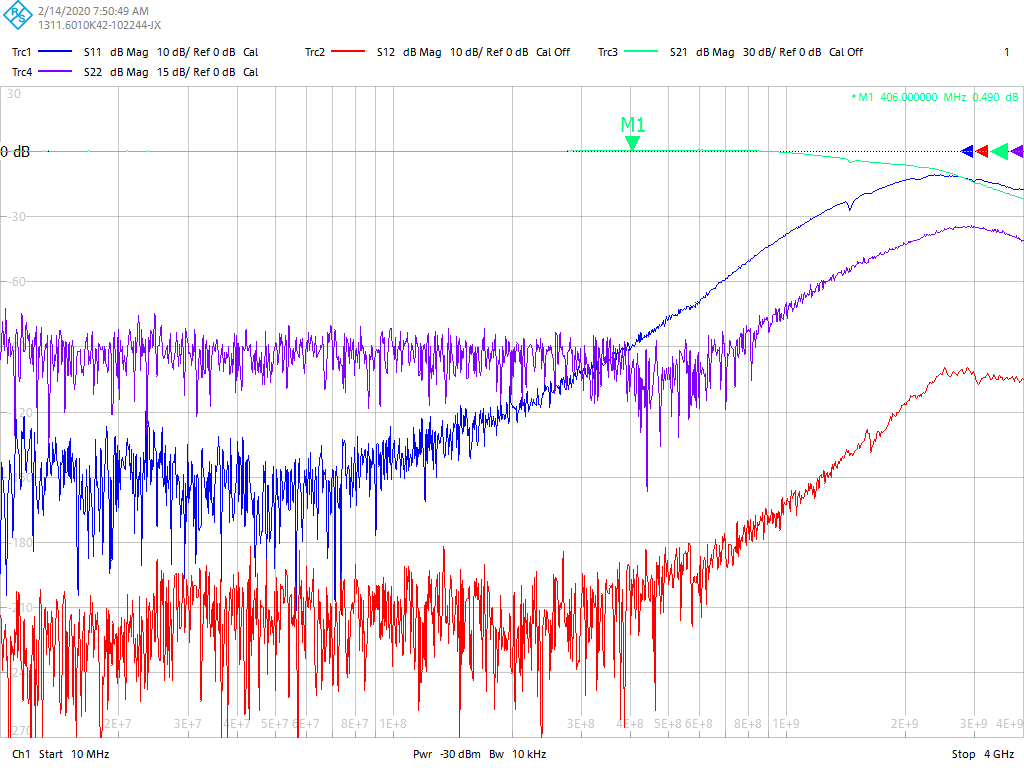
With both ICs, I have performed tests with the circuits relating to Figure 43 & 44 of the OPA858's Datasheet [Page 14], with an input signal of -30dBm. In the tests I've performed last week, the feedback resistor across the amplifier [R2] has been changed from 464ohms, up to 1K5ohms.
As a course of checking the setup, I've tried them with 2 different Network Analysers, and rebuilt the boards several times, including replacing the ICs, yet the results remain the same.
Is our test setup correct [see: attached photo], and are we measuring the right things?
- To detail the test setup, we are using a Rhode & Schwarz ZNB 8 Vector Network Analyser, calibrated to TOSM with an SMA 50ohm calibration kit, sweeping from 10MHz to 4GHz, and measuring standard S-Parameters.
[spoiler]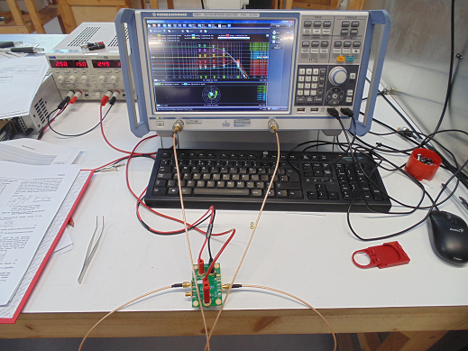
[/spoiler]
Bench Test setup
[spoiler]

[/spoiler]
[As Figure 44. OPA858 Datasheet, Inverting configuration]
[spoiler]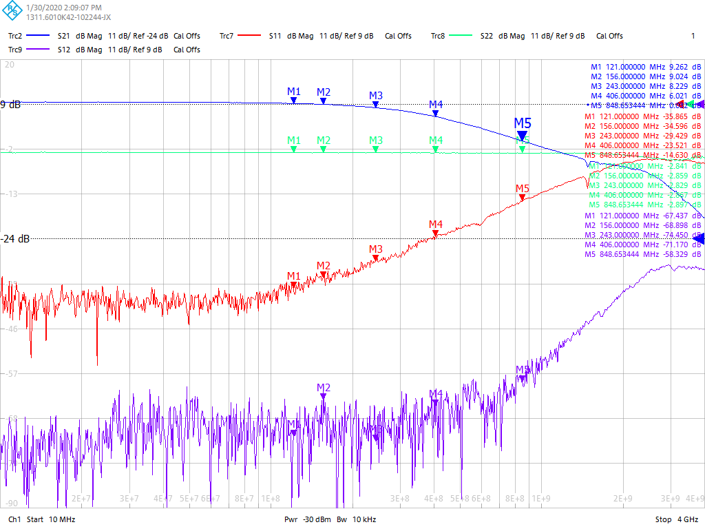
[As Figure 43. OPA858 Datasheet, NonInverting configuration with R2 as 464ohm]
[/spoiler]
[spoiler]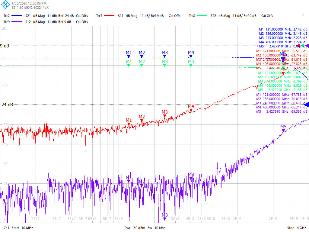
[As Figure 43. OPA858 Datasheet, NonInverting configuration with R2 as 464ohm, using OPA855 instead]
[/spoiler]