This thread has been locked.

If you have a related question, please click the "Ask a related question" button in the top right corner. The newly created question will be automatically linked to this question.

OPA388: OPA388IDBVT

Part Number: OPA388
Other Parts Discussed in Thread: TLV3201, OPA320

Hello Team,

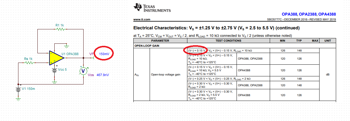
We are using OPA388IDBVT Op-amp as unity gain voltage follower and see an issue with output when we feed clock signal at input (Sine wave).

We see a variation of around 0.5Hz on 2KHz input signal at output when we do the thermal cycling from +25 to -30 C. In this case, Op-amp is powered on and error observed during ramp down condition. After stabilizing at -30C, we are not seeing this error.

Please help us by sharing the Thermal Coefficient of input offset voltage drift, input offset current drift and input bias current drift for OPA388IDBVT.

Also share the Thermal shock response curve for this device.

  • Kandula,

    Few comments here: the best is to show the circuit instead of describing it - a picture is worth thousand words.  I do not know what supplies you use (single or dual) and what is the Vin and Vout.  Make sure you do not violate the output range - is is 150mV from either rail.  If you use a single supply to power OPA388 in a buffer configuration, you must raiose the Vcm by at least 150mV so the output is within the specifed range.  Also, any source impedane at the input, Rs, must be balanced with a matching impedance in the feedback (R1) - see below.

    0743.OPA388 Kundula.TSC

  • Hello Marek,

    Thanks for your response.

    Please find the snapshot of circuit below:

    We are using single supply as 3.3V and input is biased to 2.4V. As we have clamping diodes on path, the input will vary from 1.8V to 3V (0.6V considered as Forward voltage of Diode).

    Requesting to review the circuit and share your feedback.

    As i told in my earlier communication, we are seeing frequency drift at output of Op-amp in temperature ramp down condition (+25C to -30C). When we refer other op-amp datasheets, we found temperature coefficient of Input offset voltage drift (uV/C) but not specified for OPA388 device.

    Also requesting to help us by suggesting a way to calculate the drift in frequency with drift in Input offset voltage (as we are assuming drift in Input offset voltage is the culprit for drift in output frequency, if this is not, please suggest which parameter need to be considered).

    Thanks for your support.

    Regards,

    Ramalinga Reddy

  • Ramalinga,

    OPA388 is a chopper amplifier with a choppng frequency of around fchop=200kHz. All chopper amplifiers generate input current spikes, IB, caused by closing/opening of the front-end switches and for that reason the input impedance on both input terminals must be matched (see below) or otherwise, the variation in IB glitches over temperature will result in Vos drift. 

    The maximum Vos drift of OPA388 is specified as +/-0.05uV/C BUT this does NOT include additional drift induced by mismatched impedances discussed above.

    Having said that, considering that you use TLV3201 comparator with a maximum input voltage offset of +/-5mV,  there is no good reason to pick OPA388 with max offset 1000 times lower (+/-5uV).  Thus, I would recommend you to use instead a non-chopper amplifier, like OPA320, which will not require matching impedances shown above . 

  • Hello Marek,

    Thanks for your response and sorry for delay in responding back to you.

    I have few queries on your response as listed below:

    1. If we use OPA320, can we avoid input current spikes and which reduces the Vos Drift over temperatures? This in turn reduces the frequency variation at comparator output.

    2. could you please help us in calculating Vos drift to frequency variation at comparator output to compare with test results.

    3. You are proposing 5pF cap and 100K resistor at unity gain op-amp feedback path. Is this for matching the impedance at op-amp input?

    4. Current our design is finalized and we are allowed to modify only BOM and no PCB modifications. By considering, do you have any recommendations/suggestions in improving the Comparator output frequency accuracy by doing BOM modifications.

    Thanks for your support.

    Regards,

    Ramalinga Reddy

  • Hi Ramalinga,

    Kandula Ramalinga Reddy said:
    4. Current our design is finalized and we are allowed to modify only BOM and no PCB modifications. By considering, do you have any recommendations/suggestions in improving the Comparator output frequency accuracy by doing BOM modifications.

    So, you haven't thoroughly tested the circuit?

    Kai