Other Parts Discussed in Thread: OPA192, DUAL-DIYAMP-EVM, DIYAMP-EVM, OPA2388, TINA-TI, OPA2189
Hi,
We use the OPA2192 for precise current measurement.
The first OPAMP stage is a differential amplifier with a gain of 8.333. The second and third stage form a 4th order low pass filter with a total gain of 3 and an offset of 2.048V.
All the OPAMPS are supplied with +/-5V. Please see picture 1 attached.
Now we have the problem that our current measurement shows a significant non-linearity.
The problem has been isolated to the first OPAMP stage (all measurements have been made at the output of U1).
To be able to better measure I changed the resistor values as follows:
For a gain of 1:
- R1: from 180 to 1k5
- R2: from 180 to 1k5
For a gain of 0.06818
- R1: from 180 to 22k
- R2: from 180 to 22k
How it was measured and analysed:
I always took five measurements:
1. Input voltage close to 0V
2. Input voltage close to 1/4 of the range
3. Input voltage close to 1/2 of the range
4. Input voltage close to 3/4 of the range
5. Input voltage close to full range
Input voltage range was choosen so that the maximum ouput voltage of the first stange is always 0...0.6827V (2.048V/3).
All input voltage values and measured values have been corrected with the first value. Gain was calculated with the 5th measurement.
This gain was then applied to the input voltage values to get the theoretical values that sould be at the output of the OPAMP.
Difference of the theoretical and measured values are then plotted against the input voltage values.
Results:
Picture 2 shows this for the first OPAMP stage with a gain of 1.
Picture 3 shows this for the first OPAMP stage with a gain of 0.06818
With a gain of 1 we see an max. error of approx. 0.0005V. With a gain of 0.06818 it is 0.0001V. With the original gain of 8.3333 the error is much higher.
This leads to the assumption that a higher gain has a higher max. error.
But measuring an other differential OPAMP stage (voltage measurement) that has a gain of 0.17 shows a much better linearity (max. error in the range of 0.00001V).
This stage has much higher resistor values (e.g. R10/R11 is 150k).
Can an expert for precise measurement explain what affects the linearity of a differential amplifier stage or what we are doing wrong?
An error of 0.0001V would be acceptable for the original gain of 8.3333.
Any suggestions are highly appreciated.
Thanks and best regards,
Patrick
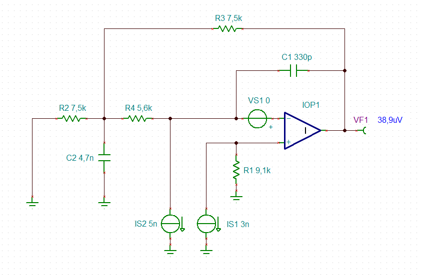
Picture 1:

Picture 2:

Picture 3: