This thread has been locked.

If you have a related question, please click the "Ask a related question" button in the top right corner. The newly created question will be automatically linked to this question.

OPA189: Using opamp to create a precision negative voltage reference. Can opamp drive decoupling caps?

Part Number: OPA189
Other Parts Discussed in Thread: ADS131E08, OPA627, OPA191, OPA378, OPA2210, OPA192, LM7705

I have a precision (0.04%) 3V reference and need to create a precision -1.7V rail from it. Note, this is for AVSS of the TI ADS131E08 ADC. I've decided to use an inverting opamp with precision resistors in the feedback. My issue is that I would really like to have decoupling caps, 0.1uF, on the AVSS pins. I'm thinking about using the OPA189. However, there is a curve showing overshoot with load capacitance. I know opamps can have issues driving capacitive loads. I'm not using the amplifier to drive "signals" but rather a DC conversion. Do I have to worry about this overshoot curve? I can't add series resistor prior to the decoupling because I can't handle any voltage drop on the -1.7V rail. Any other suggestions? Are there opamps that don't have capacitive load restrictions? Thanks!

  • Well Brett this issue comes up all the time, where there are good options, 

    There is a very sophisticated dual op amp structure used in a lot of the SAR reference buffer circuits, and then there is also the dual loop (I call it the imbedded integrator) to drive decoupling caps. I think I touched on both in this article, but this coming from much earlier material. 

    https://www.planetanalog.com/stability-issues-and-resolutions-for-high-speed-voltage-feedback-op-amps-insight-6/

  • Hi Brett,

    Do you have to use precision -1.7V rail? How much current do you need to sink per the application? Can you use negative LDO for your application? 

    You mentioned "I can't add series resistor prior to the decoupling because I can't handle any voltage drop on the -1.7V rail". One of the method is to place Rsio inside of Op Amp' feedback loop. The method will compensate the IR drop across the resistor in series at the output of an Op Amp. 

    Most op amps don't like to drive large capacitive load, because it creates a second pole that will interfere with the closed loop stability. The Transconductance amplifier (voltage in, current out) is the only one that can drive capacitive load.  

    Anyway, if you send me a schematic about your -1.7V circuit, I can help you to compensate the circuit per the application. 

    Best,

    Raymond

  • Hi Brett,

    must AVSS be so much precise at all? I wouldn't do that. An OPAmp circuit for providing AVSS can make problems with the supply voltages' sequencing by introducing a turn-on delay during power-up.

    I would take a voltage regulator for that task. They are built for that and they allow a proper power-up and power-down sequencing.

    Kai

  • Hi Everyone, thanks for the replies. Let me give you just a little more background. I'm actually using two of the TI ADS131E08 ADCs because I'm doing 11 measurements that must be simultaneously sampled. The IN-N for each channel MUST be tied to circuit ground because of the detection circuitry. Eight of the signals range from 0 to 350mV and three of the signals range from 0 to just under 3V. My measurements must be accurate to better than 0.3%.  My Vref is a precision (0.04%) 3V reference tied between VREFP and VREFN. VREFN is tied to ground. The prototype had issues because my AVSS was ground and the common mode range was violated. My solution is to change AVSS to -1.7V. In a separate TI thread I was told that VREFN and AVSS must be tied together. (Note, if this wasn't the case then I would be done because I would create a reasonable toleranced -1.7V rail and have VREFN tied to ground.) The issue is that now I must have a precision -1.7V rail since it makes up part of my Vref. I've prototyped it and it works but with the rework there are a bunch of white wires and I'm picking up noise on AVSS. I created the AVSS with an inverting opamp (TI OPA191) configuration using precision resistors. This is a pretty common method. The problem is that I can't decouple the -1.7V rail because of opamp stability as we have discussed. Note, I put a 0.1uF decoupling cap on the rail and it crushed the noise and drastically improved performance. The opamp seems to be OK but I can't move forward with that when I respin the board. There is a good chance that the -1.7V rail will be "clean" once it is properly put down on the PCB without any real decoupling.

    Michael - I will look at your link. I believe the second option you mention, "imbedded integrator", is probably what Raymond is talking about.

    Raymond - I have to use a precision -1.7V rail because of what I mentioned above. It makes up part of my VREF. I couldn't find any negative precision voltage references. I just started looking at the option of placing the Rsio inside the Opamp feedback loop. Any help you could provide (schematic and component values) would be greatly appreciated. The -1.7V rail needs to support the current draw from two ADS131E08. The datasheet says 5.8mA typical so multiply by two and add some margin. I'm thinking the total will be less than 20mA. Below is my currently proposed circuit. Note, the -3V rail is created from the 3.3V rail and isn't super precise but doesn't need to be.

  • You are correct Brett - that imbedded integrator is what Raymond is talking about - I pulled it out of the apps section of the venerable OPA627 and re-worked the equations a little - the RC solution equations are in that article. It should give you what you want. 

  • Hi Brett,

    The image did not go through. please reload. 

    Best,

    Raymond

  • I couldn't figure out how to cut-n-paste the pic in so I put it in a Word doc and attached that file. Let me know if you still can't get at it.

    I'm not using a buffer amp (using the inverting configuration) so I'm not sure how the "loop" changes to get the Riso inside. It would be great if you could show me the schematic and component values to use. I'm reading Michael's article and I was looking at the app section of the OPA191 datasheet. It shows only a buffer configuration but shows a 10ohm Riso with 1uF decoupling has good margin and very little overshoot (60 deg with 8% overshoot). It seems if I put more load capacitance it allows for lower Riso value and helps with the phase margin. I would love to put a 10uF decoupling cap in parallel with like 4-6 0.1uF decoupling caps in the circuit.

    Thank you again for the support!!

  • Go to where equation 1&2 are with figure 8 

    If you need a better copy of this I can insert a pdf - Planet analog broke the links to expand the figures, 

  • ...oh also let me know if there is a better TI opamp to use in the inverting opamp configuration. I'm not married to the OPA191. I like the OPA378 but my rails are +3.3V and -3V and it can't handle that wide of a supply range. The opamp needs low offset voltage so that doesn't impact the accuracy of the -1.7V rail too much.

  • I was wondering about that Brett 

    1st thing will be the max load current it needs to support - that DC level will set an IR drop in the inside the loop Rx resistor. 

  • Hey Michael. I can see the equations and the schematic.

    (1) That is for a non-inverting configuration. Do the equations change for the inverting configuration? Do I still place Cf and Rx in the same exact locations?

    (2) You mention that you select the F3dB well below the GBP of the opamp. Is there a limit to how low you can go? Note, I'm not driving signals through the opamp so I really only care about DC. Your article chose 2.5MHz. What if I chose 2kHz?

    Could you attach the pdf to this link? I'd like to save it so I can reference back to it if necessary in the future. Thanks!

  • You need to have some bandwidth to provide a low output impedance over frequency to the load. Need to pick a part before proceeding too far, What DC load current do you need to support? 

    Here is my pdf of that Insight #6, there are a ton of good reference here also, It does draw on #5 a lot, so I will attach that also, that figure 4 in #5 is new and something I derived some time ago now but have not published derivation -it does work exactly for a 2nd order loop - so pretty approximate a lot of the time

    Stability Issues and Resolutions for High Speed Voltage Feedback Op Amps SSU #6 March5_2019.pdf

    2311.The SSU part 5 Stability issues for high speed op amps_introductory issues article text Feb. 2_2019.pdf

  • The ADCs, which there are two of, say 5.8mA typical...so multiply by 2 and add some margin. I was thinking that 20mA would be more than enough.

  • Here are some choices, I think you really want the best DC offset part for your needs - this is ascending worst case 25C Vos. 

    That min linear Io is where the output headroom is >0.5V. 

    That OPA2210 looks like the best fit but only available in a dual it seems. 

    I would suggest we pursue the OPA192 as a solution. 

    Could you perhaps close this one as resolved (getting pretty long) and open a new one on developing a precision -1.7V supply using the OPA192 And repeat that schematic as a starting point. 

  • Incidentally Brett, 

    I have a OPA192 sim running now, the output impedance looking back in peaks to 63ohms at 470kHz, might need a faster part and/or more than the 10nF Cload I was using. 

  • Hi Brett,

    Thanks for Michael's technical assistant. It is greatly appreciated. 

    When you cut an image, please paste into Paint.exe program as png, jpeg or other formats. You click on Insert/Edit Media icon above and you can upload the image this way. 

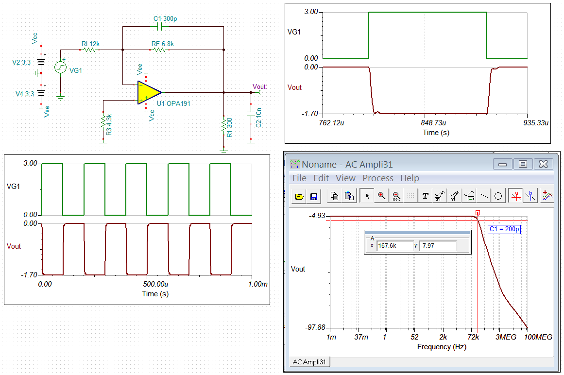
    I simulated the schematic you attached to convert 3Vdc to -1.7Vdc. Somehow you only placed 100pF capacitor as load. From the previous email, you indicated you wanted 100nF. 

    There are no issues with 100pF and 10nF capacitors as load in parallel with 300 Ohm resistor (~5.8mA). I did not follow Michael's recommendation, since the closed loop is still readily compensated with standard techniques. 

    When comes with 100nF capacitor as load, it may take some doing. However, I did not proceed since the bandwidth of the op amp is limited, which is down to 45kHz or so. If you want to pursue it, please send me a message.  It may be doable. 

    Enclosed are Tina simulation with 100pF and 10nF capacitive loads. 

    /cfs-file/__key/communityserver-discussions-components-files/14/OPA191-_2D00_1_5F00_7V-100p.TSC

    /cfs-file/__key/communityserver-discussions-components-files/14/OPA191-_2D00_1_5F00_7V-10nF-300Ohm-load.TSC

    Best,

    Raymond

  • I can definitely open a new ticket once we decide on a part. Let me know what you determine with the OPA192, Note, I can definitely add more load capacitance. Again, I was thinking 1uF or 10uF in parallel with like six 0.1uF caps.

    I do have question regarding your statement about needing "some bandwidth to provide a low output impedance over frequency to the load". The ADS131E08 (the ADC I'm using) datasheet shows an example of an external reference driver (see figure 29 on page 26) using an "In-Loop Riso" configuration which is what we are talking about...except that I'll be doing an inverting opamp and not a buffer amp. When I use the two equations from your Insight #6 paper on that circuit I get two f3dB: Equation #1 yields 1224.25Hz and Equation #2 yields 102.309Hz. That is pretty low frequency but I'm gathering that works given it is a recommended TI circuit. Note, Rx=10ohms, CL=10.1uF, Rf =100kohms and Cf=0.022uF.

  • Well actually Brett, you are treating this minus supply like it needs to be as good as a reference buffer driver. That article has an example of the imbedded driver amp circuit that comes from a couple of TI reference designs in the references

    I still wonder about this. If you only need to get to ground on the input signal, a lot of people just use the LM7705 to get a negative 0.23V supply. 

  • Hi Brett,

    I agree with Michael. Can you ask  about negative rail requirements for ADS131E08? I am not familiar with the ADC, though I recalled the negative voltage needs to be -0.3V or lower , when I check with the datasheet. 

    I am going to close this inquiry. If you need help with OPA192, please send us a new inquiry via E2E, so that these Q&A won't be mixed up. 

    Best,

    Raymond

  • The issue all started when my new board didn't work. I wasn't aware of the common mode requirement of the ADS131E08...reference section 9.3.4.1 of the datasheet. When I go through the calculations (I could attach my Excel sheet if you want), given my inputs described earlier, I need an AVSS of around -1.7V. Creating that rail as a minus supply is no problem until I posted a question about the VREFN pin on the ADC. I was hoping to keep that tied to ground but the datasheet shows VREFN to be AVSS in the electrical section. I posted a question and one of your engineers responded with YES that I need to tie the two together. As soon as I do that then the -1.7V rail becomes part of my ADC VREF and needs to be tight tolerance and low noise.

    Raymond - My schematic only had 100pF for Cload because that fell within the allowable capacitive loading. You show that 0.01uF is OK as long as I put 300ohms in parallel. However, I would like to have more load capacitance, 1 or 10uF in parallel with several 0.1uF caps, to make sure the -1.7V rail is clean.

  • Hi Brett,

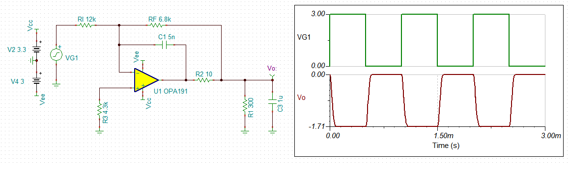
    Enclosed is OPA191 with 300Ohm load and 1uF capacitor. It looks stable with square wave. As you can see, the BW of the circuit is reduced significantly. 

    /cfs-file/__key/communityserver-discussions-components-files/14/OPA191-_2D00_1_5F00_7V-1uF-300Ohm-load-04012020.TSC

    Best,

    Raymond

  • OK. So what does that (reduced bandwidth) mean in terms of circuit performance? ...given that I'm only passing a clean DC signal through the circuit.

    Thanks for simulating it. Michael mentioned using the OPA192 because it can drive more current than the OPA191. Could you verify the simulation with the OPA192?

  • ...is the 300ohm resistor that is in parallel with the Cload there to simulate the current draw or is it required for performance? I ask because it only draws 5.7mA and I'll be drawing more (5.8mA times 2 plus some margin) and I need to know if that is a component I need to put in the final circuit.

  • Hi Brett,

    What does that (reduced bandwidth) mean in terms of circuit performance? 

    I hope that there are no power on or off sequence requirements for the application. Perhaps this is ok for the application.

    If there is a fast transient event that requires a circuit to response immediately, the lower BW circuit may not be able to response in a timely manner, or missing the fast transient event entirely. 

    Could you verify the simulation with the OPA192?

    Yes, I can do that. Please create a new E2E inquiry, since I'd like to response this in a different thread. 

    I am going to close this thread, since the initial questions have been answered. 

    Best,

    Raymond 

  • I created a new thread

  • Got it. thanks, raymond