This thread has been locked.

If you have a related question, please click the "Ask a related question" button in the top right corner. The newly created question will be automatically linked to this question.

OPA192: In-Loop Compensation Inverting Opamp configuration to create a precision -1.7V reference

Part Number: OPA192
Other Parts Discussed in Thread: ADS131E08, , OPA191, THS4551, ADS127L01, LM7705

This is related to a previous thread. I need to create a precision (better than 0.1%) -1.7V rail from a precision (0.04%) 3V rail. The -1.7V rail is feeding AVSS and VREFN for two TI ADCs, part # ADS131E08. The current draw for the two ADCs is 11.6mA typical (probably 16-20mA max). I would like to be able to provide capacitive decoupling (ideally 1uF or 10uF in parallel with 4-6 0.1uF caps) on the -1.7V rail to prevent noise.

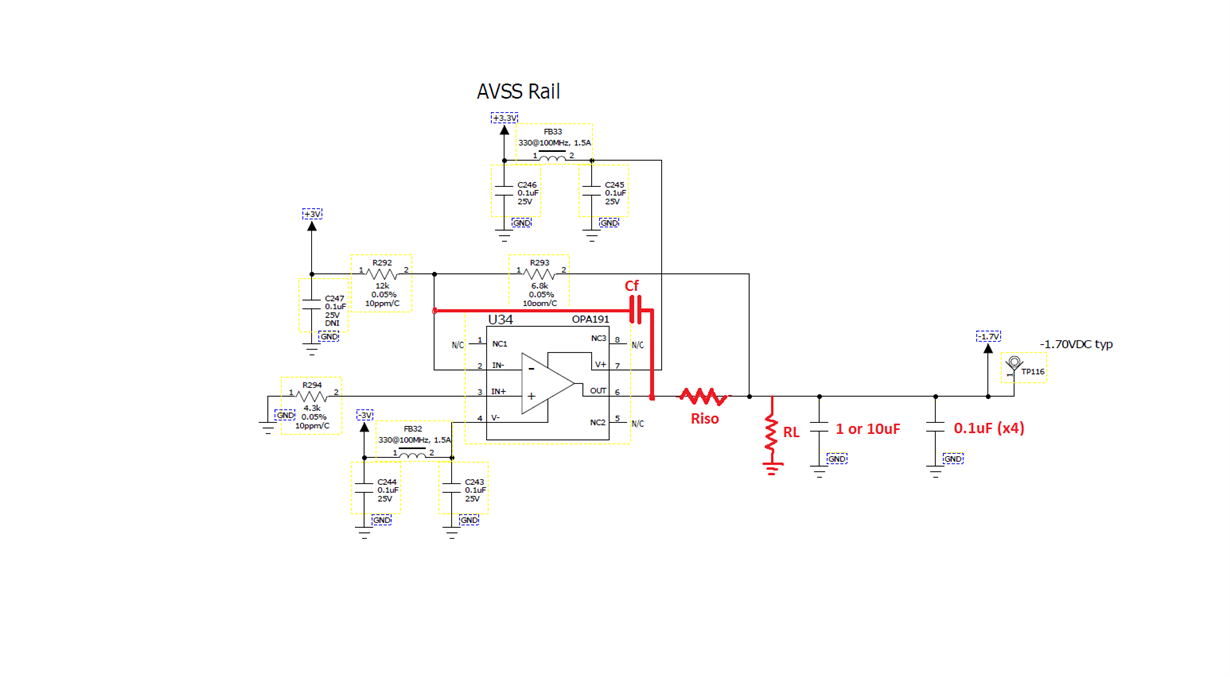
My thought is to use an OPA192 in an inverting opamp configuration with In-Loop Compensation using precision resistors. I need help verifying component values (Cf, Riso, RL), max load capacitance allowed/required, and circuit performance. See my initial schematic below.

  • Note, there is an OPA191 in my schematic because that was my initial choice. I'm leaning towards the OPA192 instead. I'm not married to it yet if you have a better option. It needs to be very low offset, low noise and capable of driving the current.

  • Hi Brett,

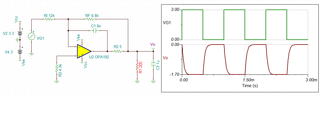
    I checked the resistive load, R1, from 80Ohm to 2kOhm and it seems to be stable. I varied the output capacitance, C3, from 1nF to 2uF and it seems to be stable. So I would say that the compensated OPA192 simulation looks pretty good. Please limit the loads within the simulated range. 

    The step voltage's edge response from 0 to -1.7V is slow at approx. 191usec. Hopefully this is good enough for your application. 

    I need to remind you that this is the simulation only. Although it looks pretty good, you have to confirm it after you put the circuit together. Since there is no oscillation, the accuracy of -1.7V should be good based on the simulation. 

    /cfs-file/__key/communityserver-discussions-components-files/14/OPA192-_2D00_1_5F00_7V-1uF-200Ohm-load-04012020.TSC

    If you have any questions, please let us know.

    Best,

    Raymond

  • Hi Raymon, hi Brett,

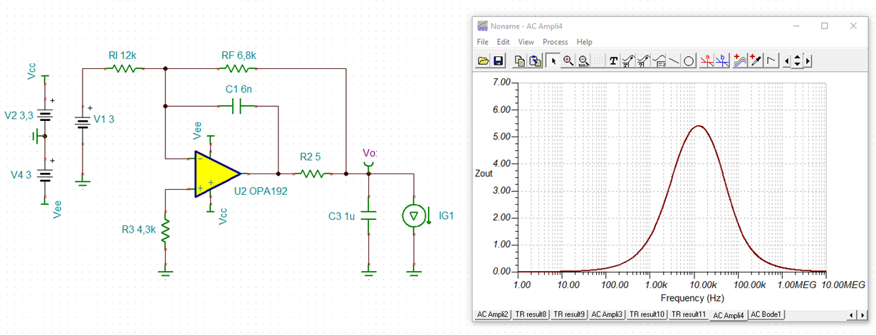
    and this will be the output impedance of the circuit:

    raymond_brett_opa192.TSC

    Kai

  • Hi Kai,

    Thanks! That is a good trick. 

    Best,

    Raymond

  • Yes Brett, this was kind of where I was thinking you needed to go, 

    Forward response looks very stable, 

    The OPA192 does not have bias current matching, so just ground your V+ input. Just adding noise with that R there, the lower curve here is that R set to zero

    And if we include the typical 3nH self resonance on the 1uF the output impedance looks like this, this is why you often parallel a 1nF with it. 

  • HI Michael,

    Thanks for the comments. I learned something from experts today. 

    Best,

    Raymond

  • Thanks guys! I think this is the best circuit for the high precision negative reference.

    However, I discovered a huge concern with the TI ADC (ADS131E08). When using a bipolar power supply, the datasheet says you have to tie the capacitors on the VCAP pins to AVSS. There is a lot of capacitance (total over 22uF) and that presents a huge load capacitance to the -1.7V power supply above. I've posted another thread asking about whether I can tie those caps to GND instead of AVSS (I think that answer will be no) or if I can use a low precision DC-DC to create the -1.7V AVSS and use the above high precision opamp -1.7V circuit to feed the VREFN pin. The issue with this second option is that the datasheet says to tie VREFN to AVSS. If I do as I have suggested they are at roughly the same voltage but they aren't directly tied to each other. I'm still waiting on someone to respond. If the answer for both options is NO then I'm screwed and will be back at the drawing board trying to determine a circuit I can use for simultaneous sampling of multiple signals with high precision.

  • So Brett I have not looked at your other threads on why you think you need a -1.7V, and you may well but it is pretty odd. 

    The ADC you quote is differential input so it transfers the differential input voltage to hold capacitors I think - most of the work done on getting to true ground with the LM7705 was with SARs. This is  a real nice national part that generates a fixed -0.23V output from a positive supply input. Often that is all need to get to ground on amplifier outputs anyway,where most of my experience is with the FDA's driving these diff input ADC's. I assisted quite a bit on the THS4551 driving the ADS127L01 sigma delta. And there is a reference design driving that in the THS4551 reference designs. 

    The easiest way to find those reference designs is to go to the design and development tab then way down on the left there is a reference designs section where if you scroll through that you will find a lot of example designs - including a real good one on the dual amplifier reference buffer circuit. One of the messages these give is the switching frequency inside the LM7705 does not find its way into the signal path - largely because that path is all differential. 

  • The reason for the negative rail is to make sure the input pseudo common mode voltage stays within the allowable range. I can play games and adjust my IN-N voltage and scale my max voltage on IN-P pin to change the required AVSS rail but it still comes out that I need a negative rail...it comes down to the fact that I need to be able to measure a 0V signal on IN-P. Then the problem becomes that the VREFN pin needs to be tied to AVSS which means it plays in to the tolerance of the reference voltage VREF (VREFP-VREVN). That LM7705, even if a -0.23V AVSS would work, is a 5% tolerance part. That isn't even close to what I need for my accuracy. Thus the reason I started this chain trying to create a high precision negative voltage rail that can drive large capacitive load and sink as high as 20mA.

  • Well if that is what you need, looks like you have one now - 

    On the decoupling cap self resonance, I meant to say we normally put like a 100nF X2Y cap in parallel - much lower L and hence higher self resonance frequency. Here is sim with an early model I had for one of those, I added a 2ohm to de-Q the higher resonances. This is a log scale where that peak is nicely rounded (op amp output impedance coming up before the 1uF is taking it down. The 1uf hits that deep null but the the rise from there is smoothed by the X2Y element and the 2ohms in series. 

    Hits a max of 5.3ohm and then at 100MHz back up to 1.36ohm. 

  • Don't have it yet. If you look up at my post on 4/2 at 3:50pm you can see that I have to be able to drive a lot of capacitance (over 22uF) because of the caps required on the ADC VCAP pins which are tied to AVSS. Still waiting for someone to respond to my other thread.

  • Hi Brett,

    Enclosed is a version of the circuit that can simulate in Tina with 22uF capacitive load, however it has some convergence issues sometimes. Please check it out with the actual circuit and see how it will perform. Perhaps it would be good for Kai or Michael to check on the circuit and comment on it. They are highly experienced experts. 

    /cfs-file/__key/communityserver-discussions-components-files/14/OPA192-_2D00_1_5F00_7V-22uF-200Ohm-load-04022020.TSC

    Best,

    Raymond

  • Hey Raymond and Michael,

    Thanks for all the help! I just figured out the proper way around this circuit design issue. I will definitely keep this negative precision voltage reference circuit in mind if I ever need one in any future designs.

    Thanks,
    Brett

  • You bet Brett, I thought you might.