This thread has been locked.

If you have a related question, please click the "Ask a related question" button in the top right corner. The newly created question will be automatically linked to this question.

Transimpedance amp with OPA355

Other Parts Discussed in Thread: OPA355

Dear All,

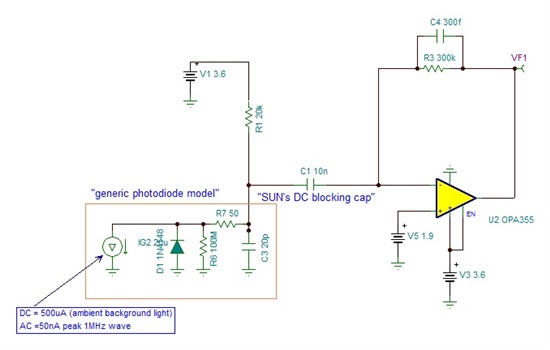
The transimpedance amp is designed with OPA355 as shown below. 

The photo detector is receiving approximately 50nA reflection signal from the laser.

Then the output voltage at VF1 is lower and lower when I increase the modulating  frequency such as 200kHz, 300kHz etc . 

When it is set to 1MHz (750nsec on and 250nsec off), the output voltage is very low and almost flat.

Is it because of opamp's low GBP?

When I observe the phase between the input signal and the output signal, there is phase shift of 150nsec.

Why there is phase delay of 150nsec between input and output?

Thanks,

Thomas


  • Thomas;

    The OPA355 should have enough bandwidth to see a 1MHz signal with no problem. There are ways that you can simplify and improve your circuit, however-- if you use the topology shown in my attached circuit, the photodiode will be reverse biased by 1/2 the supply voltage (I have made the supply voltage +5V for improved dynamic range). This is because the noninverting inpot of the op amp is biased at 1/2 of the supply voltage and the op amp feedback will force the two inputs to be equal-- therefore, the voltage across the photodiode will be 2.5V.

    I would recommend using this approach rather than a load resistor to a bias supply and AC coupling into the inverting input. You are showing 500uA of ambient background light but, to be successful, I think that you will need to put a narrow-band filter in front of the photodiode to reduce the background light by a very large factor. A good interference filter  centered on your laser wavelength and 10 to 20nm wide should do it. These can be obtained from Edmund Optics or Newport Research, etc. The DC background current causes huge offsets in the transimpedance amplifier when it is DC coupled (this problem is solved by your AC coupling) but there is a second detrimental effect that AC coupling does not solve. This is the shot noise created by the 500uA background signal. This seriously degrades the SNR of your system. A narrow optical filter will reduce the shot noise and DC offset.

    Your "Generic Photodiode Model" may be contributing to why you are having a problem. Remove the diode D1; it is not necessary since you are looking into a very low impedance input and its capacitance is adding to the total capacitance of the photodiode plus the input capacitance of the OPA355.

    OPA355 TZA 2.TSC
  • Hi Neil


    You indicate "I would recommend using this approach rather than a load resistor to a bias supply and AC coupling into the inverting input." is there a specific reason for this?


    The architecture you propose doesn't block the DC, therefore int he first stage you would be limited to a small gain, perhaps one can block the DC between first and second stage but wouldn't it better if one AC couples the PD up front and use the maximum Rf to get a high gain in the first stage?


    Thx

    Frank

  • Frank;

    For one, the 20k load resistor would not be contributing noise. Second, it is simpler. If you are worried about DC offset caused by background light, then you are not filtering the photodiode adequately. Remember that that background light current is generating shot noise.