Hi,
We are trying to build a relatively fast trans-impedance amplifier for an avalanche photo diode in an X-Ray experiment at a free-electron laser. We decided to use an LMH6629 for this purpose. After extensive simulation with TINA-TI which yielded excellent stability with a wide stability margin concerning capacitive loads, we decided to build an amplifier.
This is basically the example circuit from the datasheet of the LMH6629, but the APD is connected via JP1 and connected at the cathode rather than the anode:
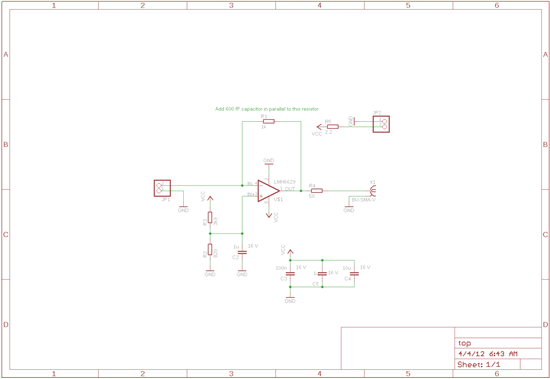
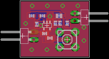
This is the respective PCB. All connections to the APD, except the APD socket, are soldered. Biasing is done on an extra PCB as we want to be able to use this amplifier with different APDs.
Though the 600 fF capacitor is not shown here, it is actually soldered on top of the 1k resistor.
Now, without any diode connected, the output of the opamp oscillates at about 750 MHz, 10 mVpp. We have built several of these and achieved about the same result, except one time, where the amplifier was actually stable. However, we have no idea why.
The same happens when we solder this board to the Diode carrier board. However, when adding the Diode to this circuit, another oscillation at 165 MHz, 50 mVpp can be seen. The Diode has a capacitance of about 4 pF when biased at 80 V.
So, now the question is of course: Do you have any hints how to get rid of this behaviour? Filtering the 750 MHz oscillation could work, but adds more complexity and does not solve the 165 MHz oscillation
Kind Regards,
Johannes
Hi Johannes,
I'm not surprised that with the APD disconnected from the LMH6629 input (and inverting input left floating), the device oscillates as it is not unity gain stable. With no APD, your closed loop gain is essentially 1 V / V which is below the 10 V / V minimum of the LMH6629 in SOT23-5 package (LLP-8 can do 4 V/V as well if the COMP pin is pulled high).
The inverting input of such a fast device (GBW= 4GHz) is very sensitive to any capacitance. I'm not sure exactly how you've implemented JP1 and the way it allows the APD to connect to the amplifier, but you want to minimize any stray capacitance that is hanging on this pin. So, it is best if for experimentation, you connect the APD to the input directly (no connectors or excess capacitance) with short direct leads. You want to start from the tightest stable configuration first in order to demonstrate feasibility before adding connectors or other things which are less ideal.
Once you minimize strays on the input, you could parallel a very small trimmer cap across the 1k feedback to allow trimming the compensation cap. The values you need are so low that you may be able to use a pair of insulated twisted wires to achieve the effect. Also, the schematic within Figure 5 allows you to get a lowered value equivalent capacitance. Figure 4, a series RC across the inputs may be additional compensation necessary in your environment. But, I'd first reduce my setup to the lowest stray state before taking other measures.
Also, be careful of how you probe the output. If necessary, isolate the typical 12pF load of a x10 scope probe by using a series resistance for isolation. On your board, eliminate ground plane around the sensitive pins. Another possibility is to order the EVALUATION board and modify it for your application. This way you can eliminate the layout as a possible culprit.
Hope these suggestions help.
Thanks,
Hooman
we have now completely redesigned our circuit to fit onto one board and added the RC filter between the inputs (180 Ohm, 10 pF). Sadly, it had nearly no effect. We now see a very sharp oscillation at about 300 MHz and 1.4 GHz. I have attached our most recent PCB.
Most interesting to see was, that the 600 fF capacitor had no effect. We got nearly the same results without it. Also, adding the pair of wires to trim the circuit, always greatly increased the amplitudes of these oscillations.
If you have any additional ideas, please let me know. I have attached our PCB, the Diode is directly soldered into it.
Best Regards,
Dear,
I think you should keep in mind, LMH6629 is not unity gain stable OPA, that's a key. You can use OPA820 to try again. Remember, OPA820's Vcc=5~12V if single supply is applied.
Hope my English word can help. My first language is Chinese.
Yes, I think, we will try using another operational amplifier. Thank you for your help. :)
Here are my comments in no particular order:
Hope this helps.
Hello, can you explain the 90 Mhz limit, i dont understund, if the GBWP is 4 Ghz?, and when say the minimun stable gain (g = +10) if i use g = +100?
Here is what the datasheet states regarding "Constraint 2" (90MHz) that you asked about:
" “Constraint 2” places an upper limit on the feedback phase lead network frequency to make sure it is fully effective in the frequency range when loop gain approaches 0dB."
Explained differently, if the product of Rc x Cc is too small, it might only provide the necessary noise gain increase at too high a frequency to be useful! "Constraint 2" ensures that the values selected for these components is such that their effect is helpful in the frequency of interest. The full effect of a zero in the transfer function can be achieved in about a decade above it.
I'm sorry but I could not follow your 2nd point (about g= +100). Please restate it differently or provide more details so that I can respond.
Thanks,Hooman
Hello,
I need an photodiodo amplifier, the photodiode have Isc max 100 uA and cd = 40pf, and i need a Voutput max in 10 V with 200MHz band width. I believe that several steps are needed. The LMH6629 (SOT23-5), apparently has his best performance, with g = 10 and Maximum output of 200 mV, for small signal and large-signal 2 Vpp.
Could you give me a recommendation?
thank you
Can you give me your opinion about this circuit?
I have not done a complete analysis of your circuit (at least with simulation), but these things come to my mind just looking at it:
1. Using a current feedback amplifier like the LMH6703 imposes restrictions on the upper feedback resistor / gain range of the 1st stage (as you've chosen a low value of 300ohm for that). Most Transimpedance amplifiers take most of their gain in the 1st stage and for that they choose a low noise device. I think you'll not get the best possible SNR by distributing your gain in cascaded stages, as you have done. The theory is to maximize the first stage gain with a low noise device.
2. If you choose to use the LMH6703, I'd recommend the +/-5V supplies. +/-6V is the upper limit on supply voltage and leaves no margin for tolerances
If you send me the TINA schematic of your circuit we could compare the SNR / bandwidth against the ideal case of low noise / high gain input stage and then you can decide if the performance you'll get with this circuit is acceptable or not. Note that the LMH6703 TINA model includes the noise performance (including the 1/f noise region) and is accurate enough for first-pass analysis of the output noise and SNR.
0624.Photodiode I.TSC
I send the TINA file, can you recomend some sustitute for the LMH6703c?, i need 200MHz band width, with in this case Vout = 5 Vpp, i read the datasheet about transimpedance amplifier and if you want big band width you need set a low gain, is tru?, your help is good for my in this mater
thanks
eneas
I've not verified this with simulation, but if you used a low noise device on the front, you should get higher SNR. Here are a couple of possibilities which work with 10V supplies:
OPA847 (0.85nV/RtHz, 2.5pA/RtHz, 3.9GHz GBW)
LMH6624 (0.92nV/RtHz, 2.3pA/RtHz, 1.5GHz GBW)
In simulation, you'd want to increase the 1st stage Rf as high as possible, without running out of bandwidth, for best SNR. TINA already includes the LMH6624 model. For the OPA847, you could get the OPA847 Reference Design (which includes the OPA847 model) here:
http://www.ti.com/litv/tsc/sboc098c
Hi Hooman:
I have a question about the COMP pin for the LMH6629. When the LMH6629 is used for transimpedance amplifier, the gain is mostly defined by the current and feedback resistor, the output voltage is basically V=IR. Is that true? Will it change the output voltage by a factor of 10 or 4 if I connect the COMP pin to the Vcc or ground to make it 10V/V gain or 4V/V gain.
thanks,
Jason
Hi Jason,
With respect to the COMP pin:
It is best to think of this pin not in terms of closed loop gain but what it does to the open loop transfer function. With COMP pin High, your have higher bandwidth because the response reaches higher in frequency and vice versa for COMP pin Low voltage. So, when it comes to the stability of the transimpedance amplifier (which is always a challenge), you would want to be mindful of the open loop transfer function shift with COMP pin, shown below, and what you need to do to stabilize the loop.
Figure 15 in the datasheet shows the relationship between the open loop response and external compensation across RF graphically.
Regards,
Thanks Hooman, it's clear to me now.
regards