This thread has been locked.

If you have a related question, please click the "Ask a related question" button in the top right corner. The newly created question will be automatically linked to this question.

High Speed Analog Opamps for Clock Fanout

Other Parts Discussed in Thread: THS3202, THS3202EVM

Hello!

We have one high speed clock source upto 200MHZ. Our plan is to fan out single CLOCK to 2 with high speed analog opamps.

The clock distribution devices are ruled as we need the clk oputput to follow the levels of the input hence the need for OPAMPS. Can you please reccomend some high speed OPAMPS that I can use to fan out my one 200MHZ clock to 2?

The levels we are looking at is 0V-5V.

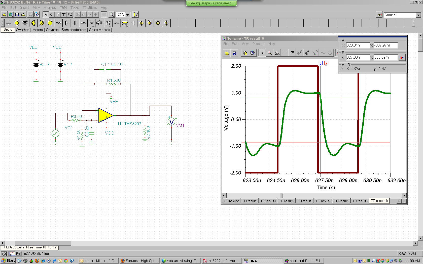
I have mocked up some simulation models using TH3202 with +/-7.5V supply and for 200MHZ clock input at the output I observe a rise time of 1nS.... (assuming no parasitics) with input parasitics of 2pF the signal integrity is lost with high rise time.

Arjun

  • Hi Arjun,

    Where are you placing the 2pF input parasitic that you mention? With 2pF on the non-inverting input in a buffer configuration, I get an output rise time of about 0.4ns (not 1ns).

    If you are adding the 2pF on the inverting node, that does seem excessive for a 2GHz device! The TINA model for the device includes the inherent capacitances already.

    I've also attached my TINA simulation file for reference:

    5444.THS3202 Buffer Rise Time 10_16_12.TSC

    What is the nature of the load (2x) that  you're driving?

    Regards,

    Hooman

  • Hello Hooman,


    Thanks for spending time on this. Here is what I have simulated... 4530.clk_fanout.TSC

  • Hi Arjun,

    To be fair, most of your rise time at VF1 and VF2 are due to the RC low pass filter (e.g. R9, and C4) at the output, regardless of how fast THS3202 transitions. You can get most of it back if you can add C5 across R9 for feed-forward. Notice the VF2 improvement over VF1:

    I also terminated the input in 50ohm and skewed your supply voltages to better accomodate the input which is entirely above ground.

    Lowering RF (currently at 650ohm) in the real application can help with speed as well.

    Please take a look:

    5125.Copy of 4530.clk_fanout-2.TSC

    Regards,

    Hooman

  • Hooman,

    I have a prototype built with this circuit and @ 200MHZ I see an overshoot at the output. For 50MHZ its works good. Its mainly due to the parasitics capacitance at the inverting terminal of the OPAMP.

    According to TINA I need to have a max parasitic capacitance of 0.1pF at the inverting terminal to not see any overshoot at the output. Do you recommend or have any suggestions as to how to keep the parastics really low down to 0.1pF? (PCB material etc) I dont have any GND plane underneath the OPAMP terminals. I just have a 650 Ohm resistor tied between Output and Inverting terminal. The resistor is as close as possible. The next thing for me to try is to place the 650 Ohm resistor on top of the device pins to eliminate any trace :).


    Arjun

  • Hi Arjun,

    I've not worked with the THS3202 specifically. Generally, I'd imagine the practical limit of lowering the input capacitance would be what is done on the EVM board:

    http://www.ti.com/tool/ths3202evm#buy

    Here I see that the ground plane is removed on all 4 layers (including the top layer) from under the sensitive components and the device pins. Additionally, you see that R6, and R1 (component tied to the inverting node) have minimal distance to the DUT pins.

    In other places, sometimes I've seen a resistor broken into 2 (or more) series resistors to reduce the apparent parasitic capacitance (at the expense of higher inductance). Resistor construction (thick film, carbon, etc.) may also affect capacitance but I'm not well versed on that subject.

    I'm not aware of any other methods of reducing capacitance beyond these.

    Regards,

    Hooman