This thread has been locked.

If you have a related question, please click the "Ask a related question" button in the top right corner. The newly created question will be automatically linked to this question.

Design Transimpedance amplifier with bootstrap under large PD capacitance situation

Other Parts Discussed in Thread: OPA847, TINA-TI, OPA842, OPA627, THS3201, THS4211, THS4271

Hi guys,

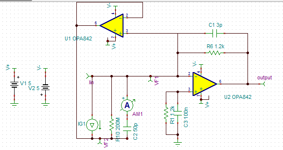
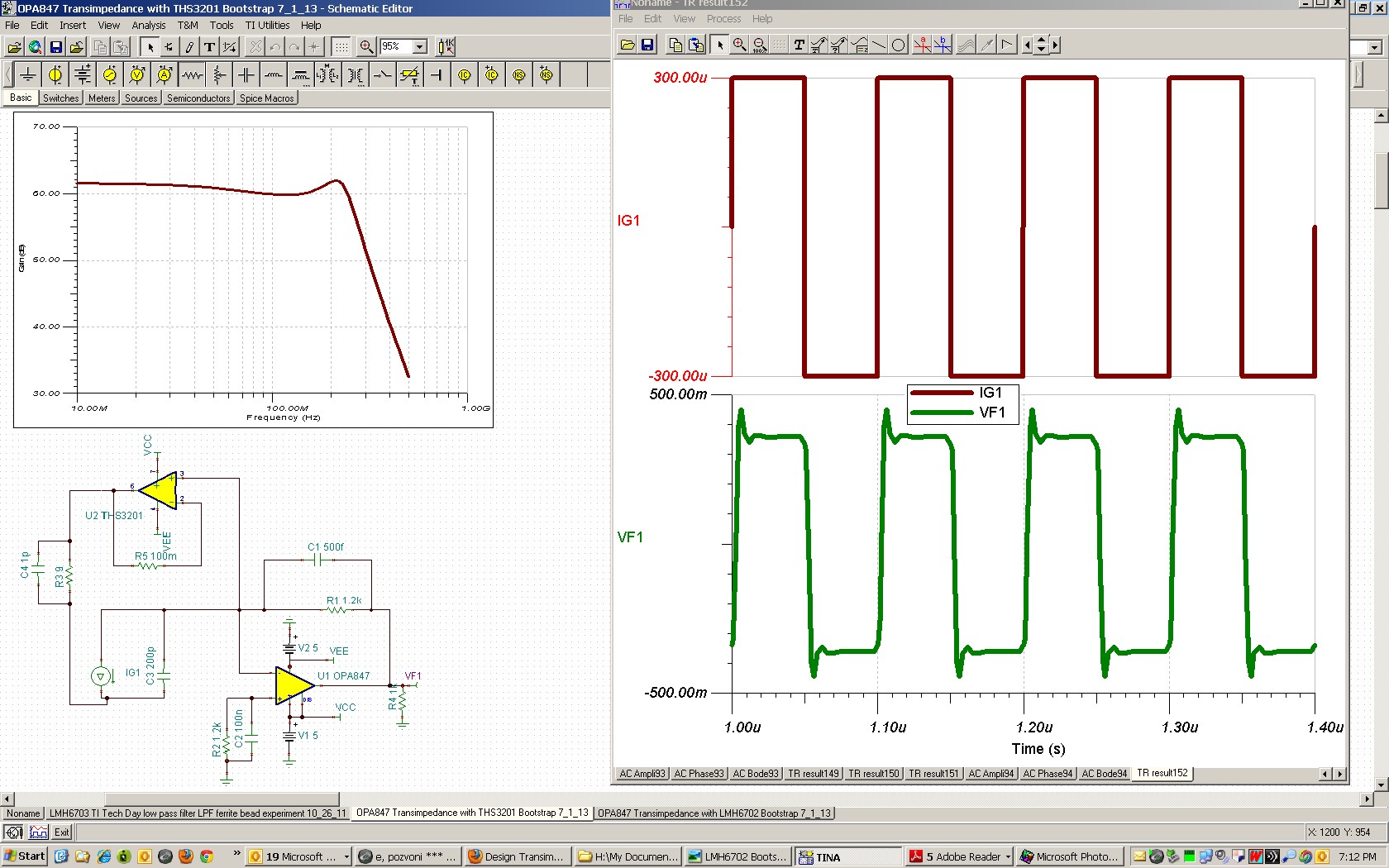
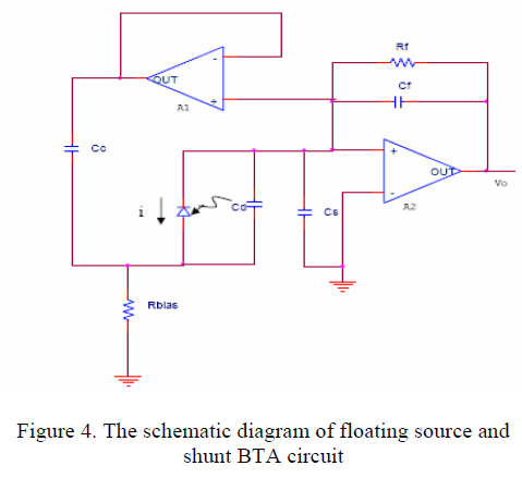
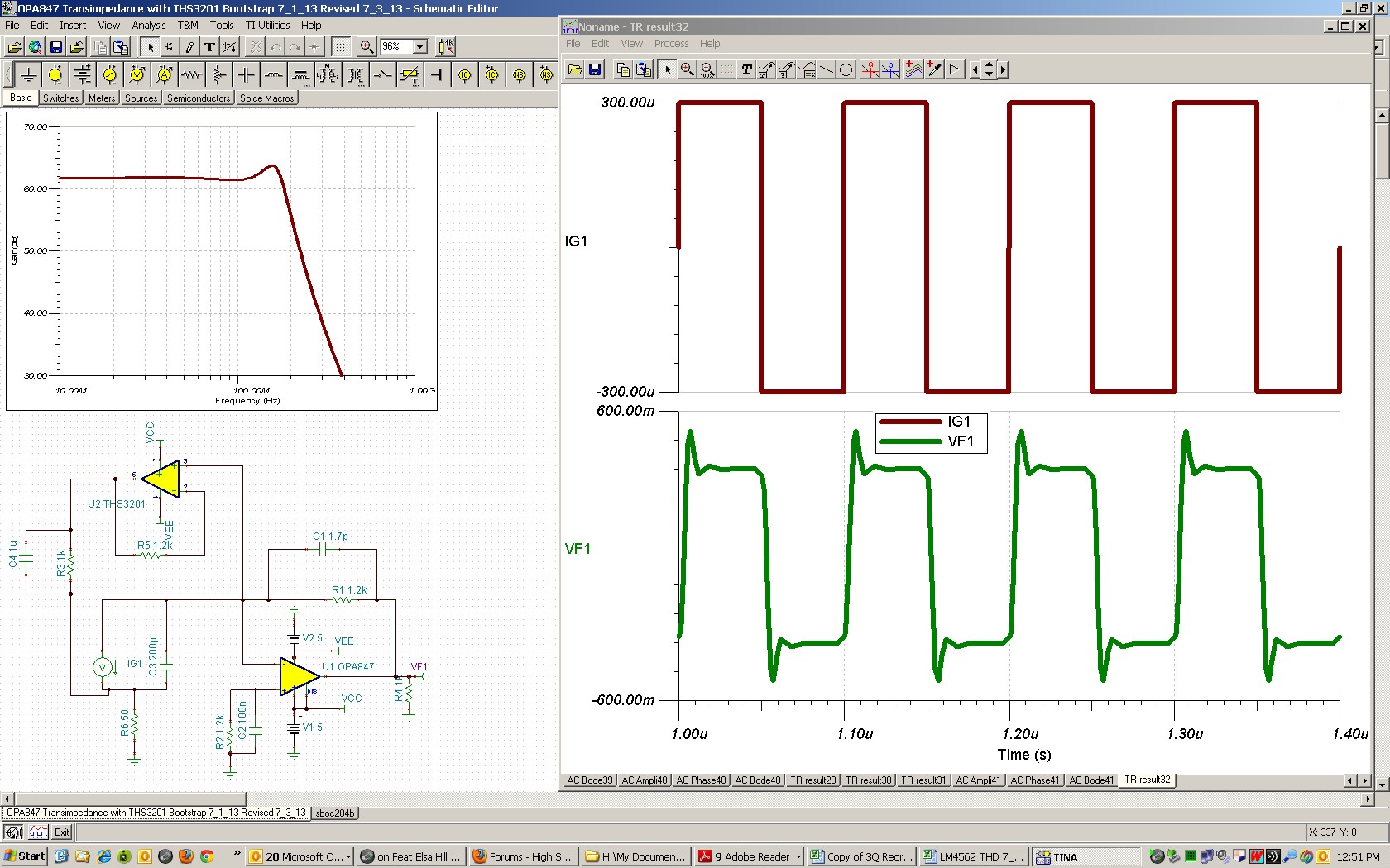
I am designing an transimpedance amplifier with an diode capacitance for nearly 50pF, and the frequency would go up to 35MHz. I used the basic topology with the OPA847 to realize the goal. However, I would like to increase the capacitance to 100pF.even 150pF if possible. while remains the bandwidth. One way that i consider is bootstrap technology. But I tried with TI components, it did not work for me.

Maybe because of the stable gain for OPA847 should not be unity. I tried the amplifier for unity gain stable as well, but it did not work either.

Could TI recommend design topology for this specific requirement? So that the bandwidth would not be affected.

Thanks very much! and I could also be reached with the email caizhch(at)gmail.com, thanks for every comment!

Jason

  • Hi Jason,

    A bit more information would be helpful here -- 

    What is your desired transimpedance gain?  Why are you trying to increase the source capacitance?  And when you say it "did not work for you", what does that mean?  Was the bandwidth too low with the increased capacitance, or was there an oscillation problem?

  • Hi Bart,

    Thanks for the reply! Currently I set the transimpedance gain to 1kohm to 1.2kohm, which is around 60db. the reason that i try to increase the source capacitance is: I am doing the photo diode array, if this TIA could be used in larger source capacitance situation, that I could use more parallel PDs to receive  more light.

    for a single OPA847 with stardard circuit, the BW could go up to about 85MHz with a feedback capacitor 2.5pF, transimpedance 1.2K, input Cap 50pF. I try to use the bootstrap tech to boost the 3db bandwidth, however, the BW didn't gain, but lost a little bit. That is why I said that. Then I tried a OPA847 and an Op amp with the open loop gain 200k, Rin 2Meg Ohm, customed op amp in TINA-TI, it still did not improve. OPA847: STABLE FOR GAINS ≥12, that's why i didnot use this as bootstrap amplifier.

    I used two OPA842 instead. the problem is the BW didn't improve. Let me see if I could post the circuit in the TINA-TI here.

    OPA842: using BTA, but problem(low Bandwidth) not solved.

    (BW:approx. 85MHz, BW goes down with the increasing capacitance, that's why i try to use bootstrapping tech to ease this problem.)

    Thanks again!

    BR,

    Jason

  • Hi Jason,

    I'm suspecting that your compensation capacitor CF (or C1 in your case shown with TINA-TI) is too large at 3pF. Going by OPA847 datasheet Equation 1 on page 11, CF= 1.8pF (with CD=~50pF). So, you might be band-limiting yourself and not realizing any benefits from the bootstrapping. . With bootstrapping (U1) you have to recalculate CF based on the OPA842 input CM capacitance since the diode capacitance will no longer be "visible" to the feedback resistor RF. You may want to try reducing CF.

    Also, I found this information on the web which has published data for use with OPA627 used as the boot strap amplifier:

    1145.OPA627 Bootstrap data 7_1_13.pdf

    Note the following:

    1. The open loop gain of the bootstrap device is important. See attachment equation 11.

    2. OPA627 is a "DieFET" input whereas OPA842 is bipolar. This may have implications for noise. See attachment Equation 12 noise calculation which has assumed no input current noise for U1.

    3. By switching from OPA847 (4GHz) to OPA842 (400MHz) you will have a speed impact. Have you tried your bootstrap arrangement with U2 (main amplifier) being OPA847 (your schematic shows it as OPA842) which has higher speed?

    Regards,

    Hooman

  • Hello Jason,

    I've given this some more thought and did some TINA-TI simulations with various bootstrap amplifier choices and found that I get instabilities unless I do additional compensation, described below. I guess it is not too surprising to see instability as you effectively have two active Op Amps within the loop and the usual additional phase shift associated with that.

    I've experimented with the bootstrap device and found that I can stabilize the loop if I use the THS3201 high speed amplifier for the bootstrap device as long as I make sure R3 and C4 are there for stability, as shown:

    With the 200pF diode assumed capacitance and with OPA847 as the main amplifier,  the simulated 3dB frequency is around 200MHz and the step response has some peaking but it is oscillation free. I'm sure the circuit would behave differently on the bench and you may have to modify the compensation employed here but this may be a starting point.

    Here is the TINA file for your reference and to see if you get the same results as me:

    8081.OPA847 Transimpedance with THS3201 Bootstrap 7_1_13.TSC

    Also note that the OPA847's slew rate (950 V/us) may start being a factor if the Photodiode current is large enough.

    Regards,

    Hooman

  • Hi Hooman!

    Many thanks to your wonderful replies and the simlulation! I have some questions with respect to the bootstrap amplifier.

    1.what are the criteria of choosing a BTA? I read before that we could use the same amplifier as the main amplifier (as long as unity-gain stable). I am aware that you use a current feedback amp THS3201, which the GBW is 1.8GHz, only half of OPA847's. Why this would not be a limit?

    2.I read some papers, which used the BTA, used a large capacitor(47nF) connecting the BTA output and the anode of the photodiode for the AC coupling.

    While you use a small capacitor parallel with a small resistor for the compensating reason. Could you give me the equivalent circuit corresponding to the circuit that you simulated? In the paper that you provided, Fig.5, the author regards va=[A1/(A1+1)]*vb, which is a follower; but I don't know how to insert that three "new" components into the previous equivalent circuit. Then I try to calculate the transfer function. And how did you get the starting values of the compensating RC circuit?

    3. How could I further improve the circuit to get better bandwidth? Apart from the optimization of the parameters of this circuit, could I introduce the common gate(JFET) topology together with this BTA? (just first thought).

    Thanks again!


    BR,

    Jason

  • Hello Jason,

    Although I'm certainly not at expert on this subject (by any stretch), I'll throw in my 2-cents:

    1. BTA Choice: From TINA-TI simulations, I know that if the BTA is slow, I run into instabilities. That tells me that I cannot have the BTA introduce additional phase shift within the passband of the main amplifier. A slower amp would have more phase shift vs. a higher speed one. That's how I came to use the THS3201 (for its high bandwidth and unity gain stability). Whatever you choose must obviously be unity gain stable or you'd have to compensate it externally for it to be stable. BTW, I had used a 0ohm feedback on the THS3201 within the simulation file which obviously won't work because it is a current feedback device (thanks for pointing that out). So, even though the simulation file I sent you looks "stable", chances are it won't be with 0ohm feedback on the bench. If you can research a unity gain amplifier that keeps up with the speed of the OPA847, I'd think that's the best choice. Also see #2 and #4 below.

    2. AC coupling the BTA: I have not researched this as thoroughly as you might have. However, using a trail-and-error technique and simulation, I've attached a TINA-TI circuit which looks promising (and this time I did use the correct feedback resistor for THS3201) below. I must note that I have not had direct experience with this.

    4477.OPA847 Transimpedance with THS3201 Bootstrap 7_1_13 Revised 7_3_13.TSC

    3. Parallel RC combination I had used: I came about these using trail-and-error in TINA-TI. My hunch was that I needed a means to control the amount of feedback to the photodiode anode. There is no guarantee that the setup would work on the bench as it seems to in simulation. I did not do any rigorous analysis for this. As mentioned in #1 above, the feedback resistor of the BTA (current amplifier) is questionable as well. I feel that the circuit does need some bench evaluation and you might gain the most if you prototype it and then we see what we need to do to stabilize things.

    4. Optimization: I feel that the BTA phase shift is currently your major limitation and what is forcing us to compensate heavily and thereby prevents you from getting the full potential of bootstrapping. A higher speed bootstrap does seem attractive based on simulation and how the BTA's lower speed (higher phase shift) seems to cause instability.

    I have seen literature discussing JFET bootstrapping techniques but I have not had experience with it myself:

    http://www.linear.com/docs/16998

    Regards,

    Hooman

  • Hi Hooman!

    sorry for the late reply! I have spent lots of time in this simulation. However, I have found out some problems and also the a basic question.

    first the basic question:

    let me post the AC simulation graph of your last schematic "4477.OPA847-Transimpedance-with-THS3201-.."

    According to the traditional control theory, we plot the 20log(A*beta) , when the gain drops to 0dB, check the phase margin. the PM should be larger than 45degrees.

    However, in TINA the ac plot above shows that the phase shift has already reached about 380degrees. Because the TINA plots the close loop? but not just A*beta? could we get the Bode plot as in the text book?

    Problem part:

    1. As I said, I simulated the schematic, but the problem that i found is NOISE. the total noise of this topology(with  200pF) has raised nearly 50times as the conventional TIA(OPA847 with 200pF) @50MHz. According to the Friss formula, the first stage is the most important, it should has the highest gain, and the lowest noise. But the bootstrap amplifier should have a gain equal or slightly less than 1. I tuned down the resistor across the BTA to increase the gain, the noise dropped but it could increase the potential unstability.

    2. According to http://www.electrooptical.net/www/frontends/frontends.pdf, figure 9. the bootstrap, the bandwidth is limited. But the noise has obviously dropped.

    the schematic:0407.TIA_35M_BFG25AX_2.TSC

    the model is also attached.1346.BFG25AX.TSM

    BR,

    Jason

  • Hi Jason,

    • Regarding your question on stability related to TINA-TI bode diagram:

    I believe you can only look at the Phase when Gain is 0dB when you are looking at Loop Gain (open loop condition). Here is what I get when I open the loop in TINA-TI by employing the large inductor and capacitor:

    Here is the TINA-TI file for the circuit above (loop open) if you like to experiment with it:

    8231.OPA847_Transimpedance_with_THS3201_Bootstrap_LoopGain_7_15_13.TSC

    • Regarding your question on noise performance of bootstrap circuit vs. traditional Transimpedance arrangement:

    I believe the difference in output noise that simulation shows is mostly due to the THS3201's inverting input current noise (20pA/RtHz) when multiplied by its feedback resistor (1.2k) or 24nV/RtHz which has some gain to OPA847 output. When I replace the THS3201 with an "ideal op amp" (from TINA-TI under Semiconductors), the output noise goes from 41nV/RtHz to 9nV/RtHz @ 1MHz. So, the THS3201's noise contribution cannot be ignored. By the way, using TINA-TI, the gain from the THS3201 output to OPA847 output is shown below and it can be as high as 43dB @ 46MHz:

    Because of this, for the Bootstrap Amplifier (BTA) it is probably advantageous to try and either use a fast, low noise JFET or the bipolar arrangement in the article that you forwarded: http://www.electrooptical.net/www/frontends/frontends.pdf instead of the THS3201. A fast, low noise, unity gain stable voltage feedback amplifier (e.g. THS4271, THS4211) could also work and have less of a noise impact.

    I tried to follow the explanation in this article for noise / bandwidth but I got a little lost. Also, the 1MHz with 100pF diode target of this article is far from your design target of 100MHz with 200pF. Also, since the final circuit performance shown in Figure 11 is unreadable, I'm not sure what results were achieved. But, the idea of a cascode amplifier in the front does look appealing (to isolate the diode from the main amplifier).

    The ideas discussed in this application note also may be applicable: http://www.linear.com/docs/16998

    I'm sorry that I'm not much help in understanding the pdf link you provided!

    Hope what I've shown helps.

    Regards,

    Hooman

  • hi Hooman,

    thanks for  replies, I will work on this issue continuously.

    BR,

    Jason

  • Hi,

    You need to AC couple the bootstrap circuit to the photo diode since the aim is to generate a suitable forcing voltage to keep the AC voltage across the source capacitance to zero.


    To find out what the suitable capacitance and the bandwidth requirements of the Bootstrapping amplifier, you need to derive the transfer function of the entire circuit and analyze by putting conditions for this scenario.


    With regards,

    AKHILESH K