This thread has been locked.

If you have a related question, please click the "Ask a related question" button in the top right corner. The newly created question will be automatically linked to this question.

THS4631 conversion issue

Other Parts Discussed in Thread: THS4631, OPA659, THS4520, TINA-TI

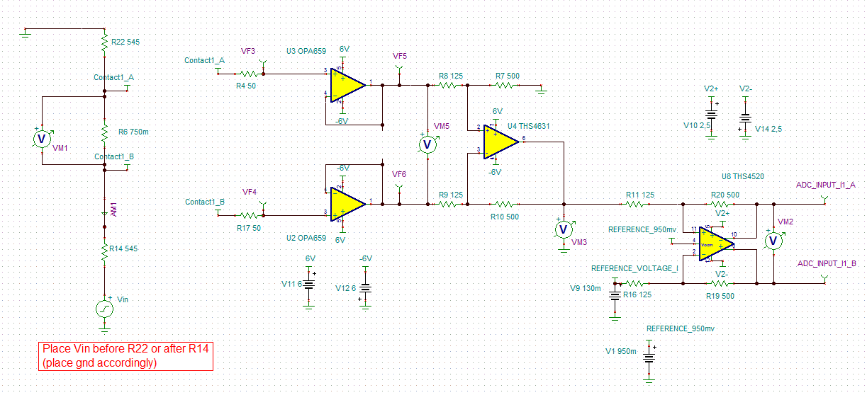
Hi I have two issue with the THS4631

I want to measure current over an resistor and convert this signal to a differential signal (needed for my ADC).

I am using two opamps (buffers) to measure the voltage over the resistor. These voltages are fed into the THS4631 (difference amplifier) and the output is fed into a fully differential opamp.

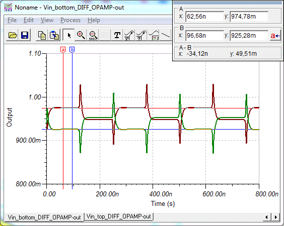
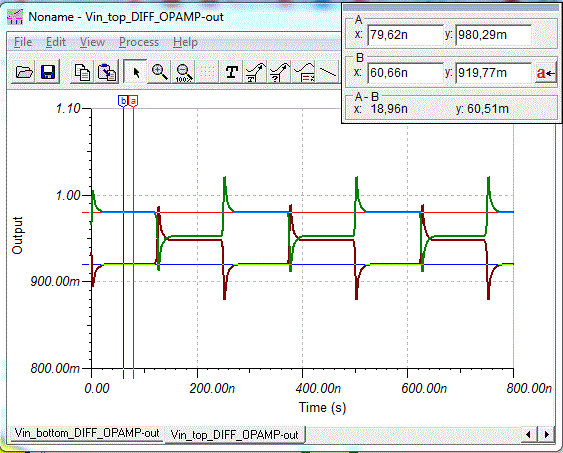
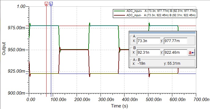
The first issue is that the THS4631 gives a different output when I reverse the current. The only change I expect is a polarity change (the current through the resistor is only reversed). Consequently the difference opamp output is also incorrect.

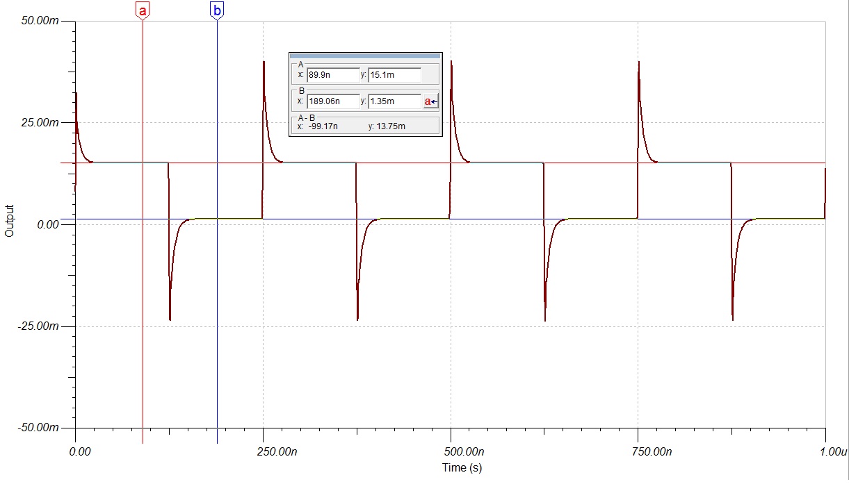
My second issue is that I see spikes at the output of the difference opamp which I also cannot explain.

Below is my circuit made in tina (I also made a PCB which behaves the same as simulated).

  • Sorry forgot to mention the input signal.

    5V clock signal (1Mhz to 12Mhz). Basically any voltage/frequency within the range is possible.

  • Hi Jozefzoon,

    Based upon the schematic provided, the buffers connected to the THS4631 are both non-inverting, due to which the signals at the input of THS4631 cancel each other when you take the difference. It would be better if you could change one of the OPA659 to non-inverting configuration.

    I have attached a schematic and signal waveform plot. I believe you are seeing something like this right?


    Thanks,

    Rohit

  • Sorry. Change one of the buffers to inverting configuration.

    Thanks,

    Rohit

  • Hi Rohit,

    Thank you for replying. 

    However this is not correct. I need to know the current through the resistor. To know this current I need the voltage difference over this resistor and the resistor value (which is known) to calculate the current. The buffers are there to isolate the measured voltages (I need a high omic load when measuring). I don't think the buffers are the issue.

    I think that I am missing something in the datasheet explaining why my next example is not correct (for a difference amplifier):

    For this example I consider my amplification 1x:

    U(+) = 1.5V and U(-) = 1V ====> U(0) = +0.5V 

    U(+) = 1V and U(-) = 1.5V ====> U(0) = -0.5V 

    This is a difference amplifiers function and this is also what I expect, only the sign is different. In my simulation, and in my PCB, this is not correct. The outputs differ.

    I hope that you understand my issue.

    Regards,

    Roy

  • Hi Jozefzoon,

    I agree with you regarding sensing the current through the resistor using OPA659 as well as the function of the difference amplifier. Based on my previous plot, the sine wave around ground is what you would see if you measure across 0.75ohm load because the voltage difference would be very small.

    Could you please post your signal waveform output plot such that I could better understand what you are seeing? 

    As far as what I am seeing based upon your schematic, I have attached my plot. So, in the plot only thing that's added is the inputs to the ADC. I would get just phase reversed signals if I connect VG1 across R1 instead of R3.

    Thanks,

    Rohit


  • Hi Rohit,

    Sorry for my late reply but I was trying to figure out why the circuit is behaving as it is.

    It appears that the buffers and difference OPAMP are functioning correctly. I isolated the issue to the fully differential OPAMP.

    I expected that the output of the fully differential OPAMP to be the same for both input scenarios, Vin at R1 (in your circuit) or Vin at R3 (in your circuit) . Again what I expect is that the output will remain the same in both cases... but inverse.

    below is are two plots I made of the output of the fully differential OPAMP

    The first plot is for Vin connected to the bottom resistor (in your case at R1).

    The second is for Vin connected to the top resistor (in your case at R3).

    I am not using a analog signal but a clock signal of 4Mhz with rise and fall times of 2ns. Clock signal is from 0 to 5V.

    Why this difference in output amplitude? If I feed this signal to a ADC one signal is within range of the ADC the other is not (when the current direction changes)

    Note: the reference voltage connected to the differential OPAMP is also 0V in my circuit (like it is in yours)

  • Hi Jozefzoon,

    Ohk. So, you are applying a square wave signal.

    The reason why you are getting differeneces in output amplitude when you change the current direction is because, you are applying two signals of equal phase but different amplitude to the difference amplifier (THS4631). 

    A difference amplifier always substracts its input. For two signals of equal phase but unqual amplitude, when the negative input (Vin-) of the difference amplifier is greater than the positive input (Vin+) of the difference amplifier, you get an output voltage less than zero because the difference is negative. Upper plot is the output of the THS4631 when clock signal is applied from the top whereas the lower plot is when clock signal is applied from the bottom. Similarly, you will get an output greater than zero if Vin+ is greater than Vin-. This happens to be the case for your setup, when you change the current direction.

    However, you would get the same voltage swing at the output of the difference amplifier, because the difference of Vin+ & Vin- inputs in both cases is the same. It can be viewed as a common mode change in the output signal of the difference amplifier which is not centered around 0V. This common mode change not centered around 0V in the output signal (for both the current directions) of THS4631, when fed to the +ve input of THS4520 (fully differential OP-AMP) will exhibit a change in output voltage swing for the two scenarios of change in current direction.

    The output voltage swing for both the cases is supposed to be 55mV. However, we get an output voltage swing of ~ 60mV and 50mV for the current from the top & bottom respectively. If you do the DC analysis in TINA for the schematic, you get different common mode voltages of 8.32mV & -5.52mV at the input of the THS4520 for the two different current scenarios.


    Thanks,

    Rohit

  • Hi Rohit,

    Thank you but I still have a hard time understanding the behavior. You are now seeing the same thing as I am. The difference OPAMP is responding as it should, correctly. It's output is in both cases (normal current and reverse current) +V or -V ( |+V| = |-V|  equally big). So far so good. I think we both agree that the difference OPAMP is not the issue, I am correct?

    If I add this +V or -V I would expect the same magnitude at the output of the differential OPAMP, or am I missing something? This should be independent of the common mode voltage of the differential OPAMP.

    Why this difference?

    Regards,

    Roy

  • Hi Roy,

    Yes. You are correct. The differential OPAMP output should be independent of the common mode voltage of the differential OPAMP.  But, the way of looking at the differential OPAMP output is incorrect. You are actually looking at the V(p-p) of two different signals and adding them up.

    You should see the V(p-p) difference for the ADC_input+ in the schematic and add that with the V(p-p) difference for the ADC_input- in the schematic. This comes out to be 55mV for both the current direction cases.

    Thanks,

    Rohit


  • Hi Roy,

    As far as the spikes in the outputs are concerned, that is because of the mismatch in the clock signal rise time at the difference amplifier (THS4631) input.  This spike is only amplified at the fully differential OP_AMP (THS4520). Also, in real world scenario, there could be mismatch in phases between the buffers OPA659 which would only worsen the spikes. Is there a specific reason why you are using a clock signal (square wave) instead of a sine wave? Square wave when sampled at the ADC input will demonstrate more spurious spectrum rather than a sine wave.

    Regards,

    Rohit


  • Hi Rohit,

    Why are the two different common mode voltages of 8.32mV & -5.52mV for the differential OPAMP (according to you)  for the two different current scenarios? Why would it matter?

    And how to make them equal.

  • Hi Roy,

    There are two different common mode voltages at the output of the (differential OPAMP) THS4631 from two different current scenarios because from the plot above,

    Vout(p-p) at THS4631 output when clock signal applied from the top = (15.1mV - 1.35mV) = 13.75mV. So, 13.75mV divided by 2 and added that with 1.35mV gives 8.22mV. Similarly, Vout(p-p) when clock signal applied from the bottom = (1.35mV - (-12.4mV)) = 13.75mV. So, 13.75mV divided by 2 and subtracted that with 1.35mV gives -5.53mV.

    It would matter because the fully differential OP-AMP (THS4520) negative input is centered around 0V, and when you apply the +ve input with this common mode offset for the two different current scenarios, the output common mode voltage at the output of the fully differential OPAMP will change as well. This results in shifting of the output up and down for the two different scenarios.

    Let me get back to you soon with a fix to this problem.

    Regards,

    Rohit

  • Hi Roy,

    I tried to work with your circuit but could not get a possible solution for the common mode shift problem. So, I modified the circuit to get a solution as close as to what you want. The top plot is for input current direction from the top and the bottom plot is for the input current direction from the bottom. You see an offset voltage of 0.3mV between the top and bottom current directions. No matter what, this cannot be eliminated because the common mode positive input voltage for OPA659 is always offset from 1.25V by 1.72mV. The TINA-TI circuit simulator shows rounds up numbers 1.2449 as 1.25V for dc analysis, but if you do the math then you figure out the offset which needs to be taken into account. However, as I said earlier, you should not see the V(p-p) between separate signals for a fully differnetial amplifier, instead look at it as the sum of V(p-p) of negative and positive outputs which is precise 55mV. If you feed this signal to a data converter, you would measure 55mV, because a data converter always takes inputs as Voltage differential peak-to-peak [ Vout-diff(p-p)].

    So, this circuit solves the problem of voltage over-range issue for the data converter as well as there are no spikes in the output. I hope this helps.

    Regards,

    Rohit

  • Hi Rohit,

    Thank you.. Your solution solves a few other issues for me as well, less different components and less power dissipation.

    I might loose one THS4520 because I need a 8x multiplication in total for this current measure. The other THS4520 can be used to measure voltage (this was not included in the circuit). The max frequency I will use is 24Mhz my amplification is 8x . This would mean that my Gain Bandwidth product is 192 Mhz (24 Mhz * 8). The device GBP is 1200Mhz so I can use only one THS4520.

    I guess measuring the input voltage is fairly easy. Feed one of the buffer outputs to a another THS4520 (and condition accordingly with the resistors).

    Can you tell me where in the datasheet I can find the offset voltages for the positive and negative common mode inputs? Iám having a hard time finding them.

    Thanks for you for support.

    Roy

  • Hi Roy,

    That's great. You can find the offset voltages for the positive and negative common mode inputs as +/- 0.25mV typical with a max variation of +/-2.5mV. This number can be found on page 5 of the datasheet for THS4520. The same can be found on page 5 for Ouput Common mode offset for CM input to be as +/-0.25mV.

    Thanks,

    Rohit