This thread has been locked.

If you have a related question, please click the "Ask a related question" button in the top right corner. The newly created question will be automatically linked to this question.

High Speed Peak Detector

Other Parts Discussed in Thread: OPA615, TINA-TI

Hi,

I need to build up a circuit to detect nsec width pulses. Naturally I found this thread:

http://e2e.ti.com/support/amplifiers/high_speed_amplifiers/f/10/t/167314.aspx?pi196062=1

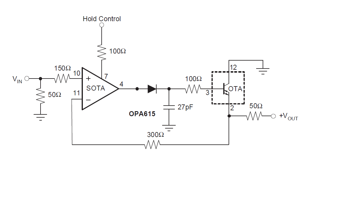
I built a circuit with reference to Fig. 48 of the OPA615 datasheet: http://www.ti.com/lit/ds/sbos299e/sbos299e.pdf

I only using the positive peak portion of the circuit.

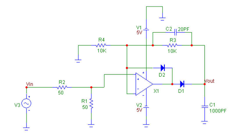
I also compared with an alternative schematic offered by the original poster:

And now are my questions finally:

1) The TI schematic in Fig. 48 looks a little strange to me, that is, the 300 ohm negative feedback resistor does not have another resistor to go to ground. Please see the alternative schematic, the R4. Why is that?

2) The 27pF capacitor in the TI schematic in Fig. 48 seem to be a little small. We found that with our proto board, the output just follows the input. I tried to increase it to 1nF and I see the output voltage starts to hold a bit. If I look at the alternative schematic, the charging capacitor is also 1000pF. So could this be explained?

3) When I increased the 27Pf to 1nF, the response time, both the rising and falling, gets bigger.

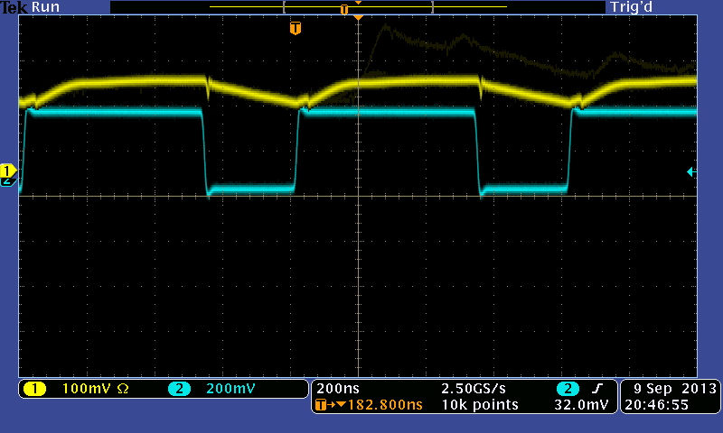
4) Anyway, I think my circuit has some problem. So here are the traces at pins #2 & #3 of the OPA615. The questins on these are:

a) the voltage relationship between #2 & #3 seem to be right, #3 (the base) should be about 0.7V above #2 (the emitter), correct?

b) what are the glitches and ringing in the traces? How do I get rid of them?

Thanks a lot,

Jay

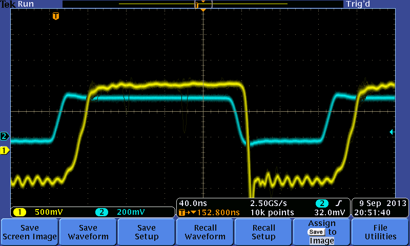
Pin #2 of OPA615 (channel #1, and channel #2 is the test signal from the sig generator):

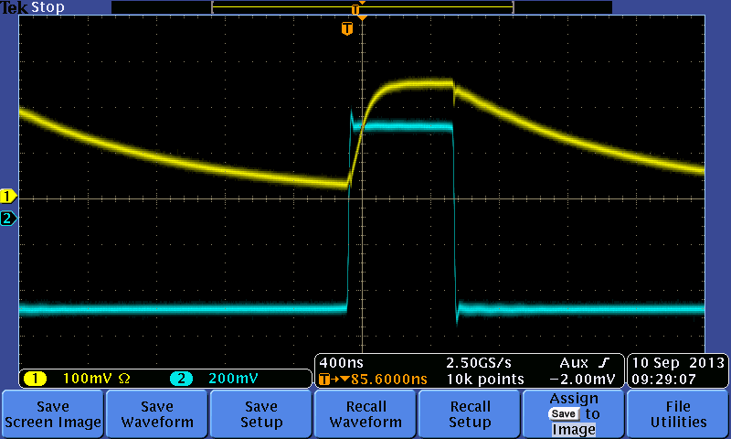
Pin #3 of OPA615(channel #1, and channel #2 is the test signal from the sig generator):

  • After using thicker wires for the inter connection, the stability of the circuit improved. However, the rising and falling time is still puzzling.

    The blue square pulse trace below of channel #2 is the input signal. The yellow trace is the output. After changing the capacitor from 27pF to 1000pF, we can see the holding and slow discharging effect. However, the rising is also slowed. When I checked the datasheet of the SOTA, I realized that it is a transconductance amplifier. So the output impedance is huge, ~ 1Mohm. As such, the time constant is about 1msec. Wait this is not right.

    Maybe I should treat it as a current source. The rise time is about a few nsec. The quiescent current is about 13mA. So charging to 0.2V on a 1000pF capacitor, t = 0.2 * 1e-9 / 13 mA = 15 nsec. OK, maybe this makes more sense. But the data seem to show ~ 200 nsec. What gives?

  • I am not a high speed amplifier expert, but I can answer a few of your questions:

    1. There is no resistor from the negative terminal of the op-amp to ground in the TI diagram, as that would cause the op-amp to amplify the input signal. Vin should be equal to pin 10. In the alternate circuit, Vin gets divided by 2 through the voltage divider consisting of R1 and R2, then the output voltage is doubled by resistors R3 and R4 (negative feedback amplification would be 1 + R3/R4 = 1 + 10k/10k = 2).

    2 & 3. It makes sense that if you increase the capacitance roughly 35x, the rise and fall time will be 35x longer. I did not do the math, but I believe 27pF is correct. 1000nF would lead to a long rise and fall time, as it would be the time constant of that capacitor and the equivalent resistance of the transistor.

    4.

    a. Correct, Vbe should be approximately 0.6/0.7V

    b. I would go through the board layout guidelines on page 23 to see what might be affecting the ringing/performance.


    I hope this clears up some confusion. If an expert could chime in to verify some of this information, that would be great.

    -Alex

  • Hi Alex,

    Thanks for the reply.

    For question #1, actually I'm not worried about the signal gets amplified. I was just not familiar with it. Maybe it's like a voltage follower, but instead of shorting the output to the input, they put in a 300 ohm resistor in the feedback.

    I know this is kind of long, but, actually I'm mostly concerned with the simple question for the OPA615, the rising and falling time. A Peak Detector output circuit by definition should be flat after detecting the incoming pulse:

    But, for the circuit I build, the output follows the pulse, and I have to increase the capacitor to prolong the voltage level. This in term dramatically increased the rising time.

    Something is not right here.

    Thanks,

    Jay

  • Also, I tried to us TINA to simulate the circuit, but OPA615 is not in the library!!

    Where can I find it??

    Thanks,

    Jay

  • Hi Jay,

    I attached a zip file containing the OPA615 TINA Macro Model (OPA615_Model.tsm) as well as a TINA schematic corresponding to the circuit you are using (first schematic in your original post, the one derived from figure 48 of the OPA615 datasheet).

    Your questions:

    1) Alex already covered that really nicely.

    2) + 3)

    Looking at the schematic in your original post (the one derived from Figure 48 from the OPA615 datasheet), you can see that the voltage at the capacitor is controlled by the SOTA. The SOTA is a sampling transconductance amplifier and has two modes of operation, controlled by the Hold Control pin. Pulling the Hold Control pin high puts the SOTA in sampling mode (output follows the input), pulling it low results in the hold mode (capacitor is disconnected from the output of the SOTA and should ideally retain the voltage present just prior to the disconnection)

    If we remove the diode at the output of the SOTA, in the sampling mode, the voltage on the capacitor is adjusted to the real-time voltage level at the analog input by charging / discharging the capacitor using the constant current output of the SOTA (voltage controlled current source). Adding the diode clamps the voltage and prevents the voltage on the capacitor from following the input entirely.

    Regarding the capacitor value: The capacitor value determines the bandwidth of the circuit. Since you would like to detect ns-pulses, you require bandwidth in the region of 100s of MHz. Increasing the cap value decreases your bandwidth. Again, assuming the SOTA is in sampling mode, the voltage at the capacitor tries to follow the input by charging / discharging the cap using a constant current (output of the SOTA being a current source). The higher the cap value, the smaller the dV / dt.

    dV / dt = I / C

    Hence, when you changed the cap to 1000pF, you decreased the bandwidth of your circuit / increased charging / discharging times. Your calculation of the time ( t = 0.2 * 1e-9 / 13 mA = 15 nsec) is correct and also treating is as a current source is correct. However, the output current of the SOTA is defined as +/-2mA (-40 to +85°C) - see the OPA615 datasheet. Using this value, it would result in t = 100ns which fits the scope screenshot you provided quite nicely.

    Using a 47pF capacitor in unity gain configuration (no gain resistor) should give you a bandwidth of around 150MHz.

    I run a TINA simulation (using the TINA file I attached) using 40ns pulses, 2V peak, 2MHz frequency. See the result below. As mentioned above, the output would naturally follow the input entirely, the diode however prevents the voltage from "falling down entirely" (clamps the voltage at a certain level).

    I hope my response could help clarify things a bit. If you have any additional questions, don't hesitate to ask!

    --Pavol

    PeakDet_OPA615.zip
  • Hi Pavol,

    Thanks for your detailed explanation. I think the key problem was the 0.7V dropoff of the diode. My Vin was simply too small and I was looking at the portion where the Vout follows the Vin. Once it dropped by 0.7V, it starts to be clamped. The Vout is very flat even with 30pF. (BTW, why the Vout goes higher with each consecutive pulses in your simulation?)

    But this 0.7V is annoying. Is there any recommended way to remove it?

    Thanks,

    Jay

  • OK, the circuit is working, kind of, and I have waveform to share. The yellow trace (channel #1) is the signal with the small pulse and the magenta trace (channel #3) is the output of the peak detector.

    It seems there is a 0.1V drop. That's good. I think I need to increase the signal amplitude, but with only about 80mV, I was able to trigger the peak detector and generate some output.

    Will work on it more, but any thoughts?

    Thanks,

    Jay

  • Hi Jay

    Did you build the circuit on the evaluation board of Ti?or did you build it some other way?

    Kind Regards

    Nico

  • I'm confused by this simulation......if this is a peak hold why does the voltage fall so much after each peak of Vin?

  • The diode chosen for Paval's simulation circuit has a zero-bias junction capacitance of 4 pF which isn't much smaller than the 27 pF capacitor. I searched for a diode with smaller junction capacitance and found a shipping Toshiba diode : 1SS427 (.3 pF). I downloaded the spice model from Toshiba's website and swapped it in the circuit. This virtually eliminated the simulated post-peak drop-off.

    Has anyone built a similarly optimized circuit and confirmed this experimentally?

    -Sam
  • I'm going to put this peak detector together and use it for 250nsec wide pulses with a peak of 3V. I need to zero out the capacitor between pulses so we are trying a couple of MOSFET 

    arrangements to see how much the affect performance.

  • I modeled the peak detector circuit in TINA and put an NPN transistor across the capacitor and drove it with a 2usec +5V pulse.

    the input photo detector pulse train was a 3V, 200nsec wide pulse followed 40 usecs latter by a 1 V 200nsec wide pulse

    The result was worryingly good with very little voltage droop. I'd like to try it with a 2N7002, but I can find it in TINA

    is there a model for it available?

  • Hi Clive,

    If there is a spice model of 2N7002 from the vendor, I think you should be able to import it in TINA-TI.

    Best Regards,

    Rohit

  • Thanks I found a model on line and used the macro wizard to upload it. It works nicely to reset my peak hold circuit.