This thread has been locked.

If you have a related question, please click the "Ask a related question" button in the top right corner. The newly created question will be automatically linked to this question.

input driver/amplifier for AD5294

Other Parts Discussed in Thread: ADS5294, THS770006, LMH6551, THS4509, LMH6554, THS4524, THS4522, THS4521, LMH6629, TINA-TI

Hello,

I want to use the ADS5294, a octal channel 80MSPS ADC.

My analog input signals amplitude is +-1V (differentiaI) @ 0V common mode voltage, and I need a DC-coupled analog input path.

Which analog input amplifier do you suggest for gain=1, that preserved the AC performance of the ADC ?

King Regards,

Niels

  • Hi Niels,

    A big challenge is the swing close to ground {0.95V(CM) - 0.5(peak_swing)V= 0.45V from ground} when using a DC coupled Fully Differential Amplifier (FDA) for this purpose, while maintaining low distortion at high frequency in the 10's of MHz!

    Here are some possibilities to do a DC coupled single ended to differential conversion for driving the ADS5294 (AVDD = 1.8V, Analog input= 2Vpp, Input CM voltage= 0.95V, 14 bit, 80MSPS ADC) analog input(s):

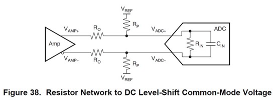
    1. CM Shift: Use a high speed FDA (e.g. THS4509, LMH6554, LMH6551, etc.) with input CM input floating (mid-supply by default) and then level shift the output to match the ADC CM of 0.95V, using a resistor network (while giving up some swing, to be made up by higher FDA gain) as shown in THS770006 datasheet, copied below:

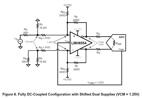
    2. Skewed Supplies: Use the FDA with skewed supply voltages (e.g. using a negative bias on the VEE of the FDA, such as +3.75V and -1.25V in the image below) to allow swings close to ground with minimal  or no impact on distortion.

    Here is an application note on this, where image below comes from:

    http://www.ti.com/lit/pdf/snoa565

    A method of generating a low negative bias is discussed here:

    http://e2e.ti.com/support/amplifiers/high_speed_amplifiers/f/10/p/170779/626965.aspx#626965


    Hope this information helps.


    Regards,

    Hooman

  • Hello Hooman,

    many thanks for your helpful answer.

    As the ADS5294 is such a low power device with 8 ADC in a small package, I wonder if there are any low power amplifers available that consume very little PCB area. Most amplifiers you suggested consume app. 3x more power than the ADC itself.

    Are there any low power dual, quad or octal amplifiers available that can be used to drive the ADS5294 inputs?

    Regards,

    Niels

  • Hi Niels,

    If you sort the FDA parametric search tool at www.ti.com  for increasing supply current, Iq,  (GBW > 40MHz, Iq < 20mA) here is what you get:

     http://www.ti.com/lsds/ti/amplifiers-linear/fully-differential-amplifier-products.page#p23typ=40;5810&columnOrderString=o1,o4,p480,p358min,p358max,p22typ,p967typ,p1max,p233typ,p1184,p1185,p512,p1182max,p517max,p1498,p1192,p2954,p1811,p1130,p23typ

    THS4521, THS4522, THS4524, LMH6551, etc.

    Here is the Excel file if you like to review it yourself:

    8171.FDA sorted by Iq 1_29_14.xlsx

    You may have to look through these devices to make sure the amplifier distortion is not a big limitation to your data acquisition, based on the highest frequency of interest where the amplifier distortion is the worst.


    Regards,

    Hooman

  • Hello again Niels,

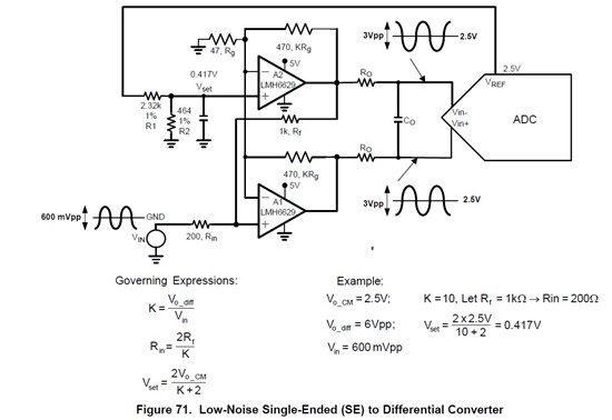
    If the FDA's in the list do not serve your purpose, you may be able to do your own single ended to differential converter using discrete op amps (which you can optimize for power dissipation which seems to be your major concern).

    The LMH6629 datasheet shows one implementation (I'm sure there are other ways), for your review:


    Regards,

    Hooman

  • Hooman,

    thanks for your help.

    Unfortunately, pcb arrea is my major concern and power dissipation is my second.
     I have to integrate 32 ADC channels in limited pcb area.

    My input signals are true differential signals with +-1V swing around 0V common mode voltage. As The product will include a user programmable digital signal processing unit, I do not know the highest frequency of interest. That's why I would like to use an amplifier that preserves the AC-performance of the ADC.

    Regards,

    Niels

  • Hi Niels,

    I'm only aware of quad FDAs (THS4524: 1.2mA/channel, 490V/us, 145MHz, RR out, ), and not Octal or other arrangement, which is probably your best bet.

    For your 14 bit ADC (ADS5294, ENOB= 12.2), the sine wave quantization SNR is:

    SQNR = 1.761 + 6.02 x ENOB

    SQNR = 75dB

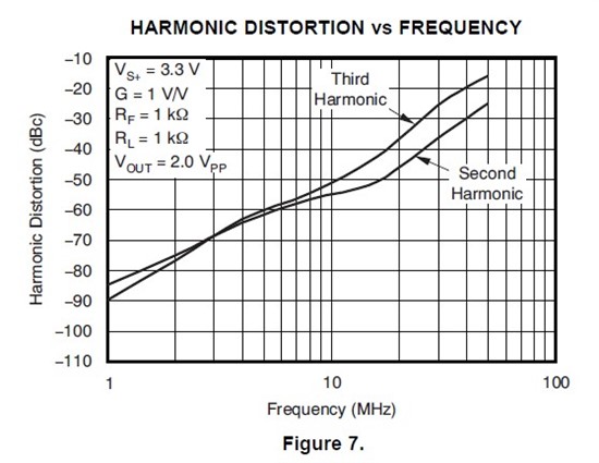
    Here is the THS4524 Distortion Plot:


    For the driver (amplifier) to not impact the ENOB, its distortion should be 3dB better than the SQNR from above. For the THS4524, you would then be limited to around 1MHz! If you can accept a degraded ENOB, then the maximum frequency can be extended accordingly. Alternatively, you would have to choose a lower distortion FDA (with the subsequent increase in its power dissipation). Texas Instruments does not currently offer any FDAs with lower distortion in dual or quad version.


    Regards,

    Hooman

  • Hooman,


    thanks for your help. 1MHz is not enough, so I will have to see how I can place all the single amplifiers and brood about how to keep them cool.

    Have a nice weekend,

    Niels

  • Hi Niels,

    I have not given this much thought yet, but:

    Can you operate the ADS5294 with skewed supplies (use -0.95V for its ground pin) so that your differential analog inputs (at 0V CM) would not need a driver and can directly drive the ADC input? This would require all kinds of level translations on the logic, etc., but it might be one way to go.

    Just a thought.

    Regards,

    Hooman

  • Hello Hooman,

    at the first glance, I shook my head when I read your idea to power the ADC with split supplies.

    But after thinking about it for a while, I would like to ask you if you have a suggestion for a power supply solution that is able to power 4 parts ADS5294.

    The resulting common mode voltage of the LVDS outputs would be app. 0V in this case?

    Regards,

    Niels

  • Hi Niels,

    I agree that the ADS5294 LVDS output CM will be very close to 0V. You still have to think about all the inputs which need to be level-shifted!

    I've presented your query to experts in Power Management, and here is what I have received so far:

    Question:

    "We have a customer who is trying to power the ADS5294 supplies (normally 1.8V single supply) off of -0.95V (VEE)  and +0.85V (VCC), for easier biasing and interfacing. Are there any DC / DC converters (for VCC and VEE both) that you would recommend?
    http://e2e.ti.com/support/amplifiers/high_speed_amplifiers/f/10/t/317742.aspx

    Each ADS5294 would consume about 620mW (77mW x 8) of power. So, that would be about 730mA output current from the VCC and the VEE converters.

    I have not been able to locate any "high current" "positive input / negative output" converters in the past. Do they exist? If not, what about a negative LDO for the VEE, if there is any that fit?"


    Responses:

    What is the input supply (I replied +3V)?  You can use an inverting buck-boost topology to generate the negative voltage.  You could probably get both voltages from a single converter using a coupled inductor, but as your output voltages are not symmetrical (I noted that symmetrical +/-0.9V will also work), you may need a custom magnetic.  See the following:

    http://www.ti.com/general/docs/lit/getliterature.tsp?baseLiteratureNumber=slva317&fileType=pdf 

    http://www.ti.com/tool/pmp5150.1

    2 normal buck converters could support this. The first could be in the usual configuration to create the +0.85V. The second could be used as an inverting buck-boost instead to create the -0.95V from the positive input.


    I will keep you in the loop if the Power Management comes out with more information useful to you.


    Regards,

    Hooman

  • Thanks.

    Do you have any suggestions for level-shifting the LVDS signals? A LVDS common mode voltage of 0.3V would be sufficient.

    Regards,

    Niels

  • Hi Niels,

    The voltage divider configuration below translates LVDS output (1.2V CM, 350mV diff voltage) to 400mV CM and terminates it for proper differential voltage. I don't know if this is what you are looking for exaclty?

    I've modeled the LVDS output as a 3.5mA peak current source (IG2) and CM components (VS2 and R2). You may be able to get away with this simple level translation that you can possibly tailor to your needs:

    Here is the TINA-TI simulation that you can tailor to you needs:

    4571.LVDS Equivalent Hooman E2E 2_12_14.TSC

    You may also be able to find a lot of information by searching "LVDS Translator" on the web, such as this link:

    http://www.eetimes.com/document.asp?doc_id=1225744


    Regards,

    Hooman

  • Hi Niels,

    For the 300mV CM you had requested, change the circuit to:

    R3= R5= 133ohm

    R4= R6= 80ohm


    Regards,

    Hooman

  • Hooman,

    thank you for your help.

    I fear that my layouter will kill me if I put all these resistors on the LVDS lines. But I will try.

    Hey, stop! I use a Kintex-7 FPGA that has build in termination resistors for each deifferential input. Perhaps I could include these chip-internal termination resistors into the common-mode-level-shifting to spare some external resistors. I will ask Xilinx.

    Regards,
    Niels

  • Hi Niels,

    Couple of points:

    1. I have not run an ADC at skewed supplies before. So, I recommend you do some more research (such as posing your question on the TI E2E for Data Converters) to verify you won't have other issues we have overlooked. HS Data Converters E2E site is here:

    http://e2e.ti.com/support/data_converters/high_speed_data_converters/default.aspx

    2. The TINA-TI arrangement I sent you yesterday on LVDS CM level translation uses 1.2V CM. If you are doing the level translations on the ADS5294 (running with -0.95V and 0.85V supplies), I'm sure the 1.2V CM level needs to be re-evaluated. I'm not entirely sure how the 1.2V LVDS CM level running with single supply comes about (if it is referenced to VEE or VCC?). So, you may have to do some homework there as well. If you have some kind of an evaluation platform / EVM, it is best to run the skewed supply conditions in the lab first.


    Regards,

    Hooman

  • Hello Hooman,

    I did an intensive research toget more information about using single supply high speed ADCs with a split supply, but with no result. Seems as if nobody has ever this.

    I asked Xilinx, and they do not recommend your level shifting scheme. But they didn't told me why.

    And last but not least, I got the information that the signal on my analog inputs has not enough power to drive the ADC inputs directly.

    So I have to swallow the bitter pill and place all these amplifiers on my board.

    Many thanks for this interesting and fruitful discussion. It was a pleasure for me.

    King Regards,

    Niels

  • Hi Niels,

    Sorry to hear that ADC power supply skew turned out to be too much of a hassle to be viable.

    Let me know if you have any questions on the input amplifier, now that you are back on that track.


    Regards,

    Hooman